Device fabrication by ink-jet printing materials into bank structures, and embossing tool

Inactive Publication Date: 2007-12-13
SEIKO EPSON CORP
View PDF11 Cites 16 Cited by
  • Summary
  • Abstract
  • Description
  • Claims
  • Application Information

AI Technical Summary

Benefits of technology

[0009] The present invention provides a fast and cheap patterning method based on depositing materials into an embossed bank structure. The technique of the present invention also reduces the occurrence of defects when printing high resolution structures. Embossing the work-piece surface to form a microstructure having at least two levels of thickness contrast enables different receiving portions of the microstructure on which different layers of functional material are deposited to have different depths. As a result, the receiving portions can be given different characteristics at particular stages of the fabrication process, to ensure that only the correct functional material is deposited on each receiving portion and to prevent the defects associated with conventional embossing techniques being formed. For example, a philic / phobic contrast can be established between different receiving portions when a given functional material is being deposited so that the functional material is attracted to the desired receiving portion and repelled from other receiving portions.
[0012] Suitably, the work-piece comprises a substrate and an embossing layer formed on the substrate, wherein the microstructure includes a stepped indentation formed in the embossing layer, the indentation having a bottom surface and a step surface, wherein the step surface is less indented into the work-piece surface than the bottom surface, and wherein the step of depositing fluid comprises: etching the work-piece surface after the step of embossing to remove the embossing layer at the bottom surface, thereby exposing a portion of the substrate surface; and performing a first treatment on the work-piece surface to create a wetting contrast between the exposed portion of the substrate surface and the other portions of the work-piece surface.
[0026] According to another aspect of the present invention, there is provided an embossing tool for creating a microstructure on a substrate, the embossing tool comprising: a first surface; and steps of at least two different heights relative to the first surface. Such an embossing tool can be used in the method of the present invention to provide a fast and cheap patterning method that avoids defects, as discussed above.

Problems solved by technology

While these techniques allow for patterning at a reasonably high resolution, the necessary tool alignment with structures that have been previously defined on a substrate presents difficulties.
Accurate alignment is especially difficult in the case of large area, flexible substrates, due to the occurrence of warping, thermal expansion or shrinking of the substrate.
Furthermore, in the case of roll-to-roll fabrication techniques, non-uniform distortions due to the tension applied to the substrate during transfer can cause further alignment difficulties.
Ink-jet printing is a very promising technique for electronic device manufacture, but the currently available free-format printing resolution (around 50 μm) is insufficient to meet the requirements of the electronics industry.
However, even using such bank structures it is difficult to fabricate electronic devices at a sufficiently high resolution without defects occurring.
However, it has been found that such embossed structures have disadvantages in many important applications.
It is difficult to ensure electrode isolation in light-emitting diode (LED) devices fabricated by printing materials onto a conventional embossed bank structure.
In addition, in thin film transistor (TFT) fabrication, reliably forming a short channel by printing material onto an embossed bank structure is a problem due to bank contamination, i.e. bridging between adjacent electrodes across a bank.

Method used


Image

  • Device fabrication by ink-jet printing materials into bank structures, and embossing tool
  • Device fabrication by ink-jet printing materials into bank structures, and embossing tool
  • Device fabrication by ink-jet printing materials into bank structures, and embossing tool

Examples


Embodiment Construction

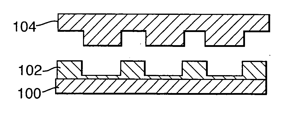
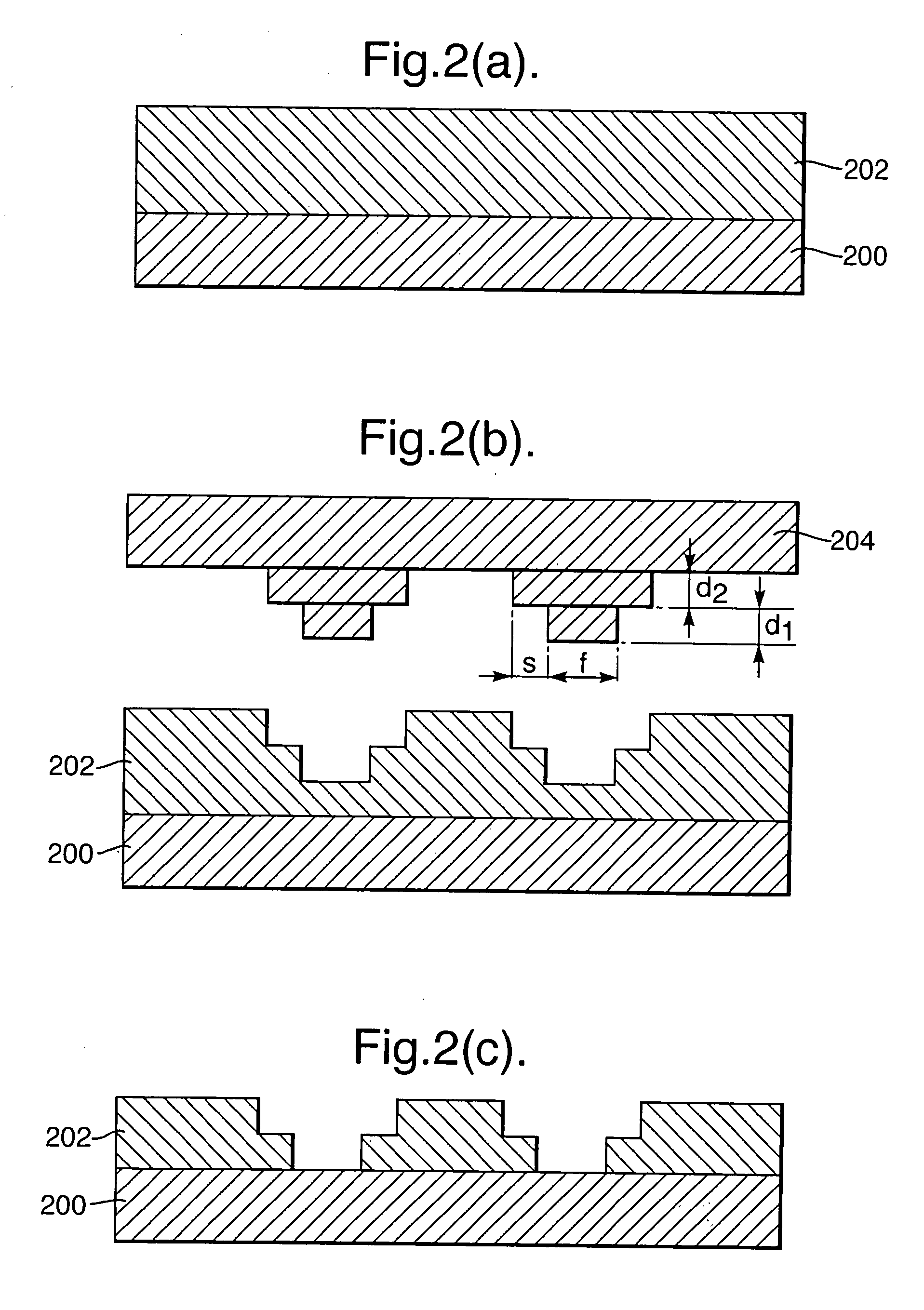
[0035] A multi-stepped tool 204 according to an embodiment of the present invention and its application are shown in FIG. 2. FIG. 2 illustrates a similar process to that shown in FIGS. 1a to 1c, comprising embossing and subsequently etching a polymer layer 202 formed on a substrate 200, but the process shown in FIG. 2 uses a two-stepped embossing tool 204. The use of a multi-stepped embossing tool provides significant advantages, as described below.

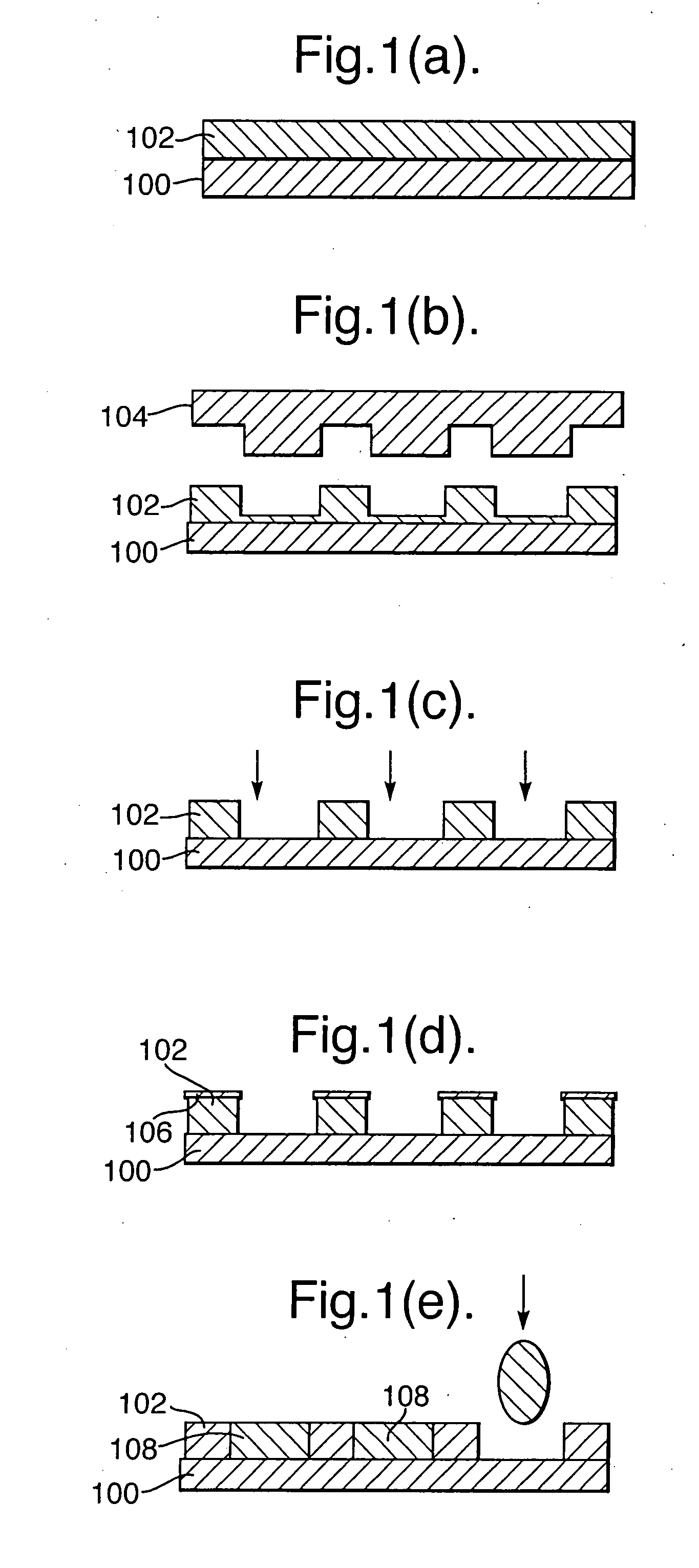
[0036]FIG. 3 shows a capacitor structure fabrication process according to an embodiment of the present invention. A 1 μm thick layer of poly(methyl methacrylate) (PMMA) 202 is spun onto a glass substrate 200 and pre-baked at 140° C. for 5 min. Then a multi-stepped silicon embossing tool 204 fabricated by optical lithography is pressed against the PMMA layer 202 at 170° C. After cooling the system to room temperature, the embossing tool 204 is released, leaving a stepped indentation in the PMMA layer 202 (FIG. 3a). The dimensions of the e...


PUM

PropertyMeasurementUnit
Thicknessaaaaaaaaaa
Microstructureaaaaaaaaaa
Heightaaaaaaaaaa

Abstract

The invention disclosed relates to the fabrication of electronic devices. A method for fabricating an electronic device is disclosed, comprising embossing a surface of a work-piece 200, 202 using an embossing tool 204, so as to form a microstructure having at least two levels of thickness contrast on the work-piece surface, and depositing fluid 208 containing a functional material onto the microstructure. In a preferred embodiment, the step of depositing fluid 208 comprises ink-jet printing. An embossing tool 204 for creating a microstructure on a work-piece 200, 202 is also disclosed, the embossing tool 204 comprising a first surface and steps of at least two different heights relative to the first surface.

Description

BACKGROUND OF THE INVENTION [0001] Electronics based on organic and inorganic solution processable materials have attracted enormous research interest in the past few decades. These materials have proven their potential for use in a wide range of applications, such as light-emitting diodes (LEDs), photovoltaic cells and thin film transistors (TFTs). Recent developments in patterning technology have further proven their potential for the manufacture of large area integrated devices on both rigid and flexible substrates. Various fabrication techniques, such as optical lithography, micro-embossing, soft-contact printing, screen printing, ink-jet printing and optical interference lithography can be employed to fabricate electronic devices. While these techniques allow for patterning at a reasonably high resolution, the necessary tool alignment with structures that have been previously defined on a substrate presents difficulties. Accurate alignment is especially difficult in the case of...

Claims


Application Information

Patent Timeline
IPC IPC(8): H01L21/203B44C1/22
CPCH01L21/0337H01L51/0005Y10T156/1039H01L2251/105H01L51/0037H10K71/135H10K85/1135H10K71/821H01L21/302H10K71/13H10K10/00H10K10/46H10K50/805H10K71/00B41M1/24B41M3/06B41J2/01
Inventor LI, SHUNPUNEWSOME, CHRISTOPHERRUSSELL, DAVIDKUGLER, THOMAS
Owner SEIKO EPSON CORP
Why Eureka
Try Eureka