

Semiconductor device and method of manufacturing semiconductor device
a semiconductor device and semiconductor technology, applied in the direction of semiconductor devices, semiconductor/solid-state device details, electrical apparatus, etc., can solve the problems of large installation space (area) and hardly compactness of conventional semiconductor devices, and achieve the effect of reducing the installation space of conventional semiconductor devices
- Summary
- Abstract
- Description
- Claims
- Application Information
AI Technical Summary
Benefits of technology
Problems solved by technology
Method used
Image

Examples
embodiment 1
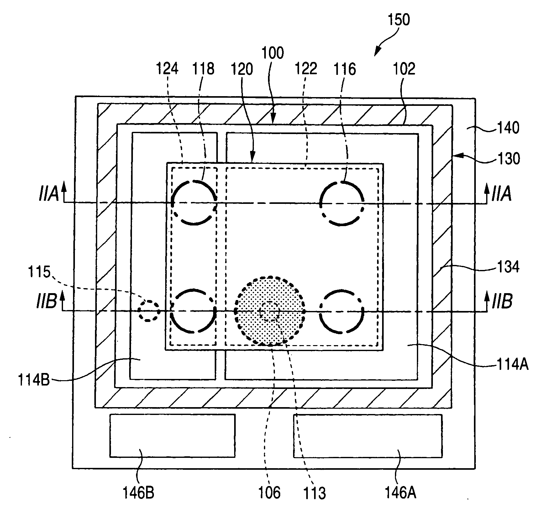
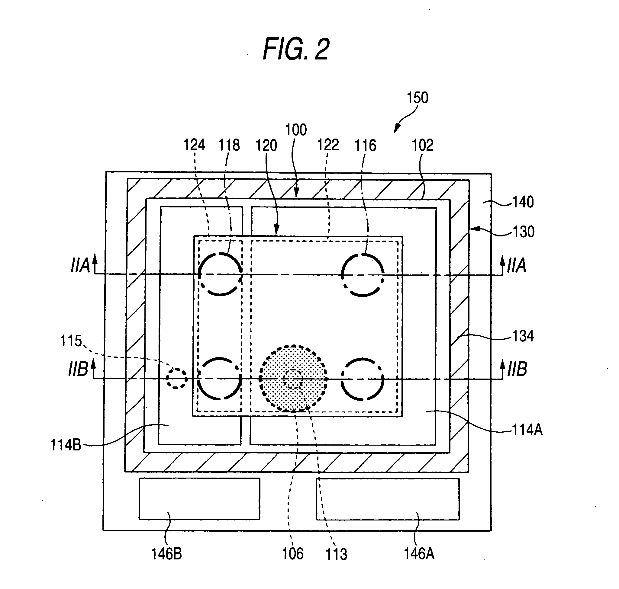
[0064]FIG. 2 is a plan view for indicating an embodiment 1 of a semiconductor device 100 according to the present invention. FIG. 3A is a longitudinal sectional view of the semiconductor device 100 taken along a line IIA-IIA shown in FIG. 2. FIG. 3B is another longitudinal sectional view of the semiconductor device 100, taken along another line IIB-IIB shown in FIG. 2. As shown in FIG. 2, FIG. 3A, and FIG. 3B, in the semiconductor device 100, a light emitting element (optical functional element) 120 constructed of an LED (light emitting diode), or the like, has been mounted on an upper plane of a semiconductor substrate 102. While the semiconductor substrate 102 has been formed by silicon (Si), a P layer 104 to which a P conductivity type impurity (for example, boron (B) etc.) has been added, and an N layer 106 have been formed in an impurity diffusion region of the semiconductor substrate 102. An N conductivity type impurity (for example, antimony, arsenic, phosphorous etc.) has be...
embodiment 2
[0099]FIG. 6A is a longitudinal sectional view for representing an embodiment 2 of a semiconductor device 200 according to the present invention. FIG. 6B is a lateral sectional view of the semiconductor device 200, taken along a line VIB-VIB shown in FIG. 6A. It should be understood that in FIG. 6A and FIG. 6B, the same reference numerals of the above-described embodiment 1 will be employed as those for denoting the same structural elements, and descriptions thereof are omitted.
[0100] As shown in FIG. 6A, and FIG. 6B, in the semiconductor device 200, a light emitting element 120 constructed of an LED (light emitting diode), or the like, has been mounted on an upper plane of a semiconductor substrate 102. In the semiconductor substrate 102, a P layer 104 to which a P conductivity type impurity has been added, and an N layer 106 have been formed, while an N conductivity type impurity has been implanted to the P layer 104 and has been diffused so as to constitute the N layer 106. The ...
embodiment 3
[0111]FIG. 7A is a longitudinal sectional view for representing an embodiment 3 of a semiconductor device 300 according to the present invention. FIG. 7B is a lateral sectional view of the semiconductor device 300, taken along a line VIIB-VIIB shown in FIG. 7A. It should be understood that in FIG. 7A and FIG. 7B, the same reference numerals of the above-described embodiments 1 and 2 will be employed as those for denoting the same structural elements, and descriptions thereof are omitted.
[0112] As indicated in FIG. 7A and FIG. 7B, in the semiconductor device 300 of the embodiment 3, an N layer 106 and an N layer connecting portion 113 have been formed in the vicinity of a center of an upper plane of the semiconductor substrate 102. Then, a region where the N layer 106 is formed is provided on the side of a mounting plane (namely, upper plane side shown in FIG. 7A) on which the light emitting element 120 is mounted, and has been formed in the vicinity of a left-sided peripheral porti...
PUM
 Abstract
Description
Claims
Application Information