
Semiconductor package having dimpled plate interconnections

a technology of dimpled plates and semiconductor devices, applied in the direction of semiconductor devices, semiconductor/solid-state device details, electrical apparatus, etc., can solve the problems of low contribution of electrical and thermal resistance of semiconductor devices to the package, the spread of solder bumps during heating and creating undesirable shapes, etc., to achieve the effect of improving thermal dissipation

Active Publication Date: 2007-12-20
ALPHA & OMEGA SEMICON INC
View PDF34 Cites 58 Cited by
  • Summary
  • Abstract
  • Description
  • Claims
  • Application Information

AI Technical Summary

Benefits of technology

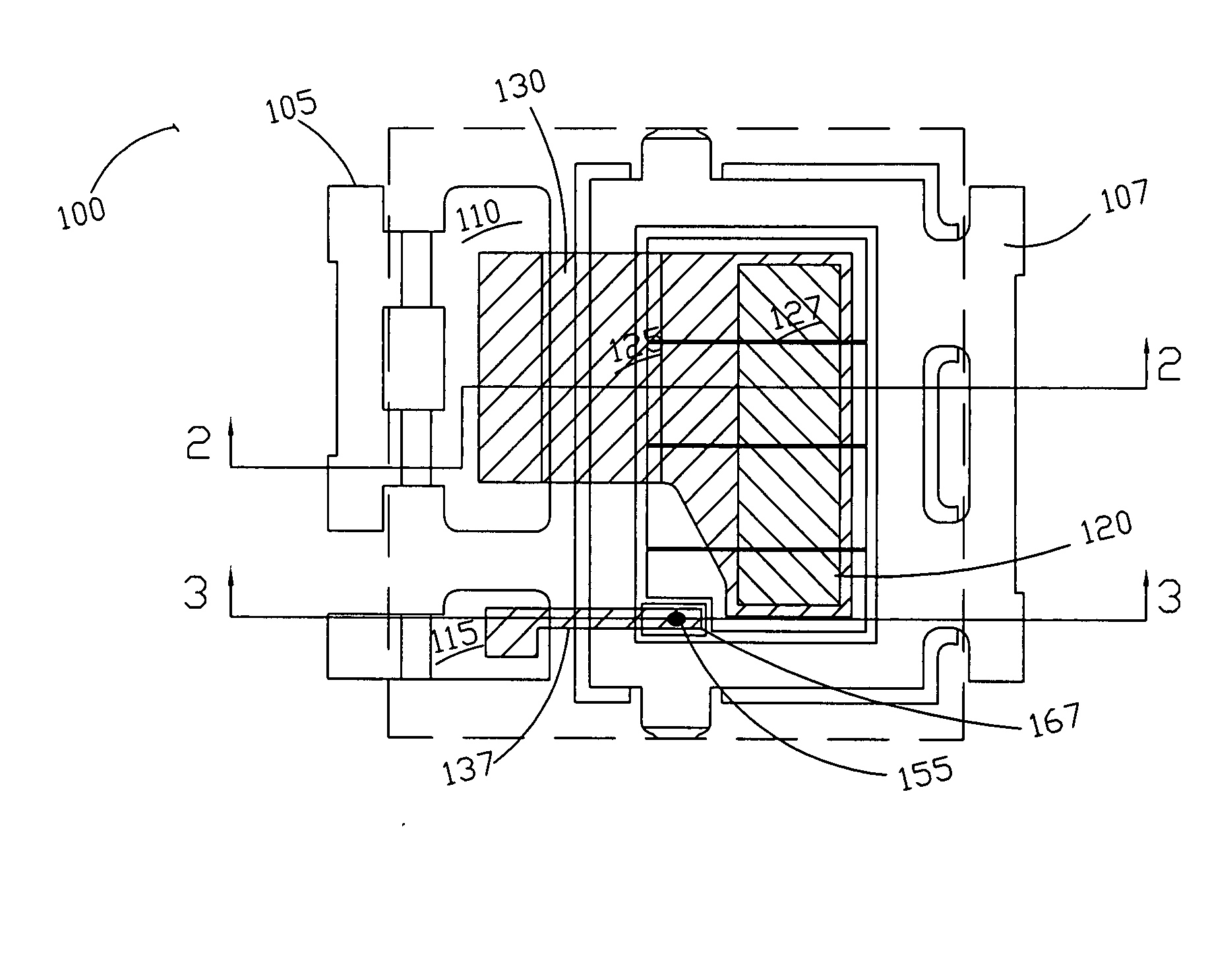
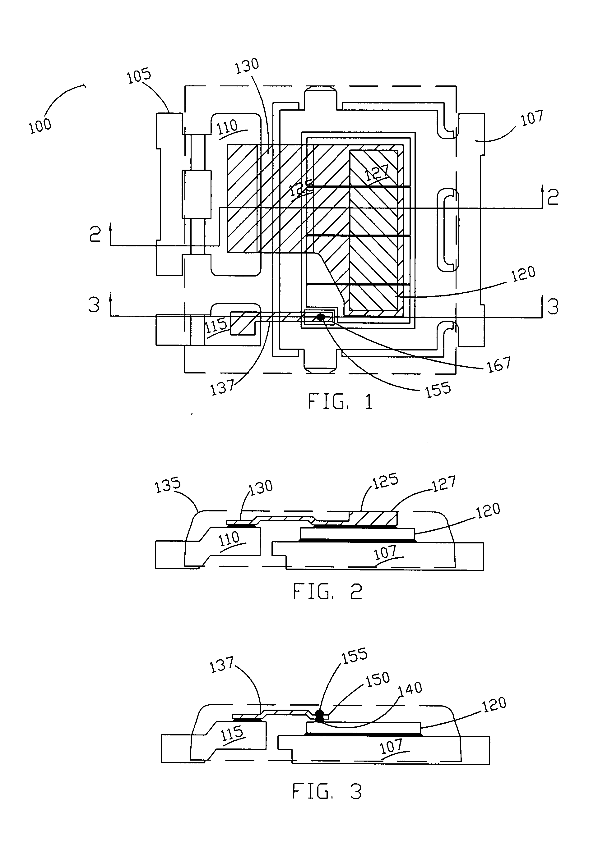
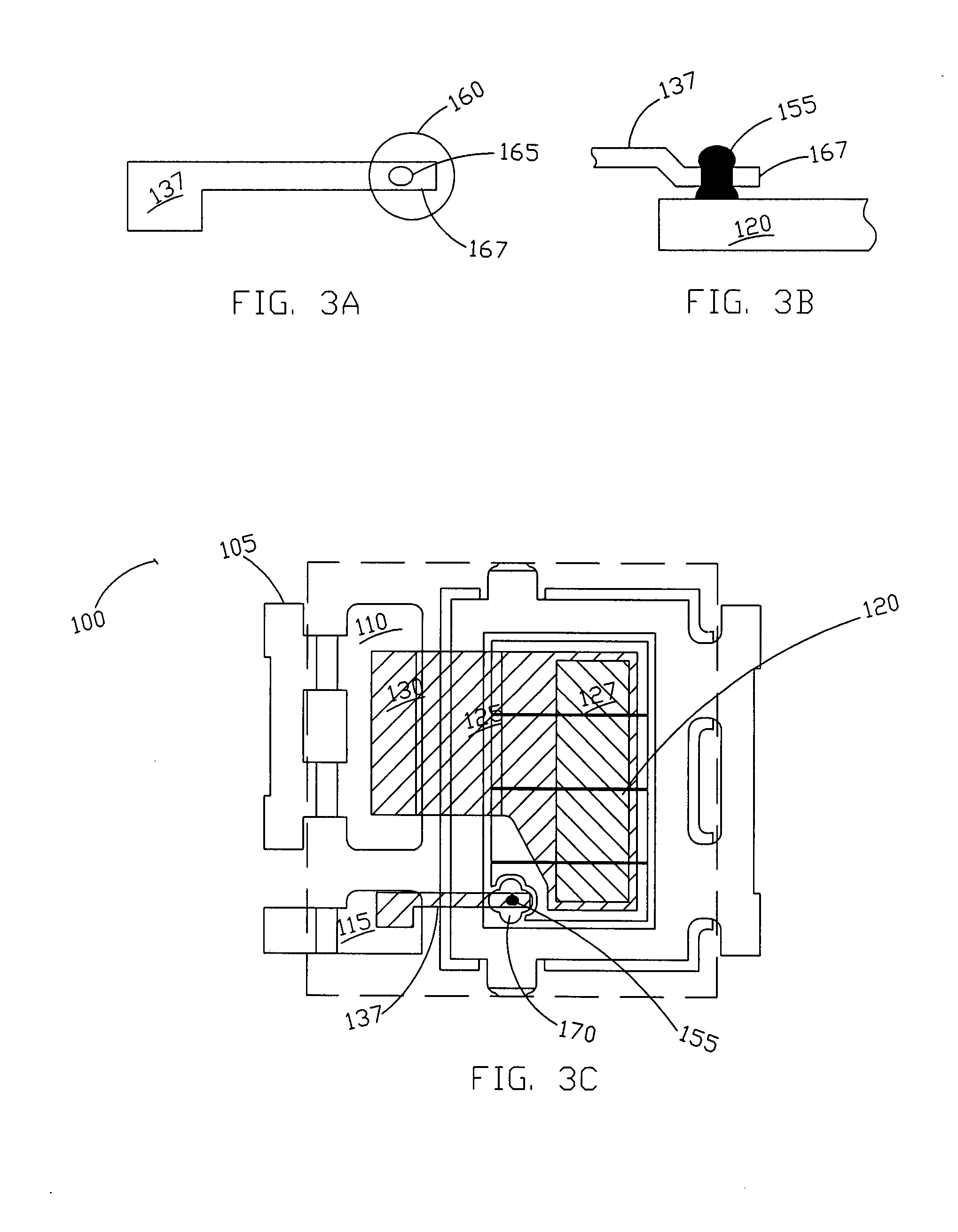
[0010] The present invention overcomes the limitations of the prior art by providing a semiconductor device package having plate connections between leadframe source and gate contact areas and a power semiconductor power device source and gate metalized areas. The plate connections include dimples positioned to correspond to the source and gate metalized areas. A portion of the source plate may be exposed to allow for improved thermal dissipation.

Problems solved by technology

The leads are alloyed to the electrode bumps in a heating furnace and the solder bumps may spread during heating and create undesirable shapes.
Wire bonding may introduce short circuits in the device due to device dialectric layer damage during the wire bonding process.
The semiconductor device has low electrical and thermal resistance contributions from the package due to the direct connection of the lead assemblies to the chip.
A common problem encountered in the use of patterned plate or clip interconnections is that the plates or clips may float during solder reflow and result in a misaligned interconnection.
In some cases, the misalignment results in a short circuit between the source and gate contact areas resulting in low assembly yields.
Furthermore, it is difficult to control the required solder volume to prevent this problem.
Another problem resulting from the use of patterned plate or clip interconnections is the thermal expansion mismatch between the silicon of the semiconductor device and the metal of the patterned plate or clip.
The larger the contact area of the patterned plate or clip, the higher the stress induced by the mismatch, which often results in die cracking.
However, the smaller contact area may result in higher resistance.

Method used


Image

  • Semiconductor package having dimpled plate interconnections
  • Semiconductor package having dimpled plate interconnections
  • Semiconductor package having dimpled plate interconnections

Examples


Embodiment Construction

[0038] The following detailed description is of the best modes of carrying out the invention. The description is not to be taken in a limiting sense, but is made merely for the purpose of illustrating the general principles of the invention, since the scope of the invention is best defined by the appended claims.

[0039] The present invention generally provides a semiconductor device package having plate connections between leadframe source and gate contact areas and power semiconductor power device metalized source and gate areas. The metalized source and gate areas are preferably Ni / Au plated or sputtered surfaces. The metalized source and gate areas provide for improved bonding of the plate connections and reduction of overbonding which often introduces short circuit problems due to dielectric layer damage during wire bonding processes. The metalized source and gate areas further eliminate the need for solder bumps and epoxy adhesive layers as soft solder and solder paste may be u...


PUM


Abstract

A semiconductor package is disclosed. The package includes a leadframe having drain, source and gate leads, a semiconductor die coupled to the leadframe, the semiconductor die having a plurality of metalized source areas and a metalized gate area, a patterned source connection having a plurality of dimples formed thereon coupling the source lead to the semiconductor die metalized source areas, a patterned gate connection having a dimple formed thereon coupling the gate lead to the semiconductor die metalized gate area, a semiconductor die drain area coupled to the drain lead, and an encapsulant covering at least a portion of the semiconductor die and drain, source and gate leads.

Description

CROSS REFERENCE TO RELATED APPLICATIONS [0001] The present invention is a continuation-in-part application which claims priority under 35 U.S.C. 120 from Ser. No. 11 / 226,913 filed on Sep. 13, 2005 entitled “Semiconductor Package Having Plate Interconnections”, the entire specification of which is incorporated herein by reference.BACKGROUND OF THE INVENTION [0002] The present invention generally relates to a semiconductor package and more particularly to a semiconductor package having dimpled plate interconnections between power semiconductor device source and gate metalized areas and leadframe source and gate leads. [0003] Semiconductor devices are conventionally connected to leadframe leads using either plate interconnections or wire bonding. For example, U.S. Pat. No. 5,821,611 discloses a semiconductor device which comprises a first lead having a tip formed with an island, a semiconductor chip unit mounted on the island of the first lead by means of a solder layer and having a pl...

Claims


Application Information

Patent Timeline
Patent Type & Authority Applications(United States)
IPC IPC(8): H01L23/48
CPCH01L2924/30107H01L23/49524H01L2924/1306H01L23/49562H01L24/36H01L24/40H01L24/41H01L2924/01013H01L2924/01033H01L2924/01078H01L2924/01079H01L2924/01082H01L2924/13091H01L2924/01005H01L2924/01006H01L2924/01047H01L2924/01055H01L2924/014H01L2224/37011H01L2224/32245H01L2224/73265H01L2224/40249H01L2924/00H01L2224/40095H01L2224/4103H01L2924/181H01L2224/40245H01L24/37H01L2224/4007H01L2224/84801H01L2224/83801H01L2924/00014H01L2224/84345H01L2224/37013H01L2224/0603H01L24/84H01L2924/00012H01L2224/37099
Inventor SUN, MINGSHI, LEILIU, KAI
Owner ALPHA & OMEGA SEMICON INC
Learn More