

Pb-free Sn-based material, wiring conductor, terminal connecting assembly, and Pb-free solder alloy
a technology of sn-based materials and terminals, which is applied in the direction of insulating conductors, conductive layers on insulating supports, cables, etc., can solve the problems of ineffective techniques for solving this problem, the mechanism of generating whisker and suppressing it is not understood precisely, and the effect of reducing the stress generated
- Summary
- Abstract
- Description
- Claims
- Application Information
AI Technical Summary
Benefits of technology
Problems solved by technology
Method used
Image

Examples
Embodiment Construction
[0062]Preferred embodiments according to the present invention will be explained in detail hereinafter by referring to the appended drawings.
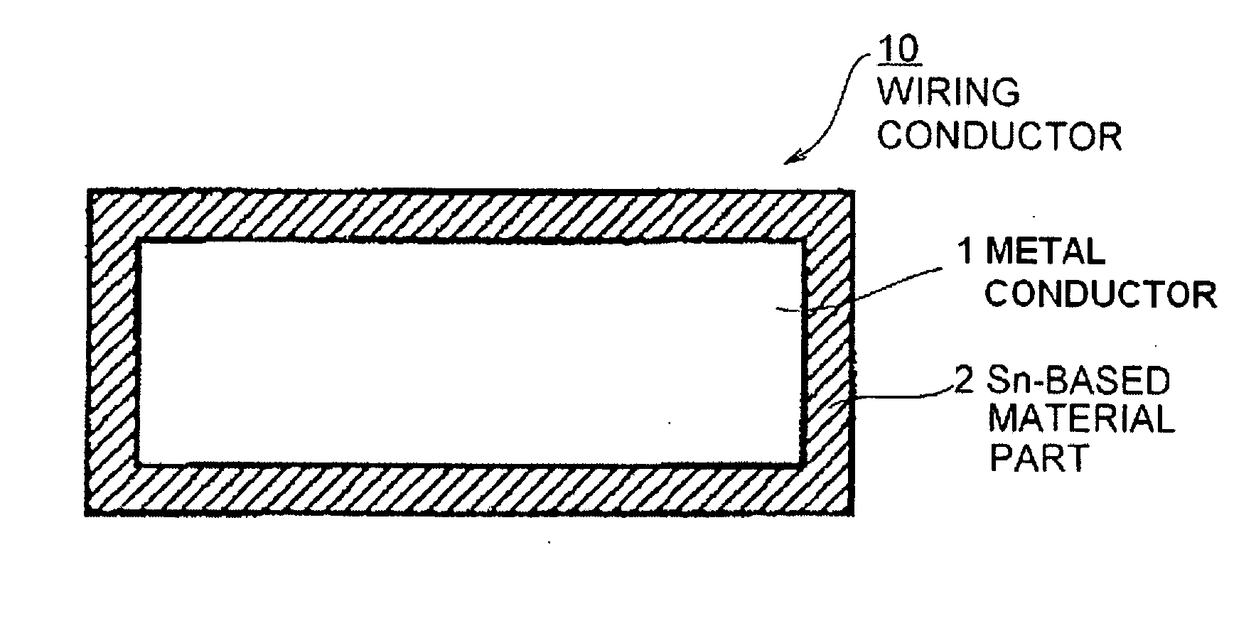
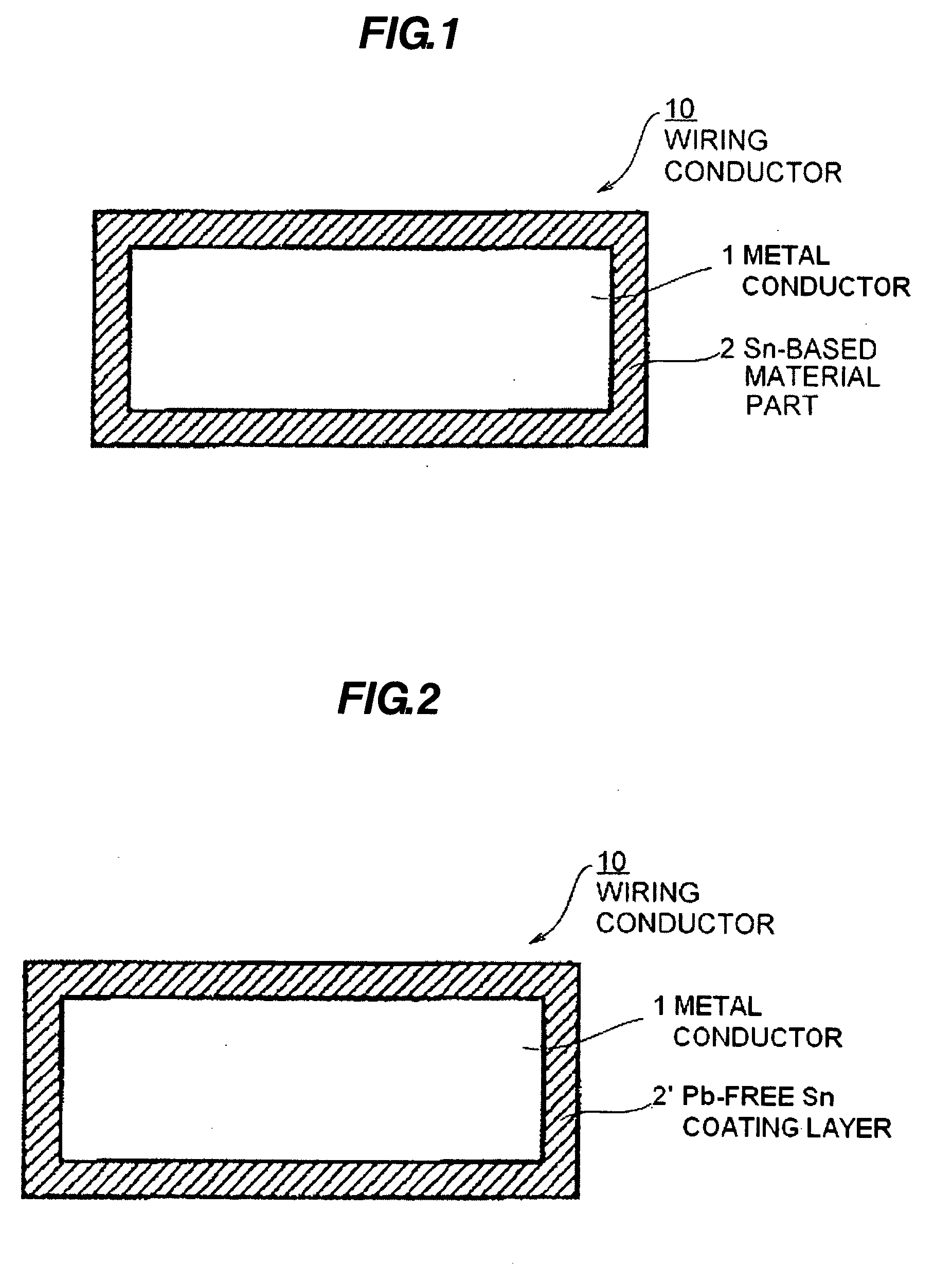
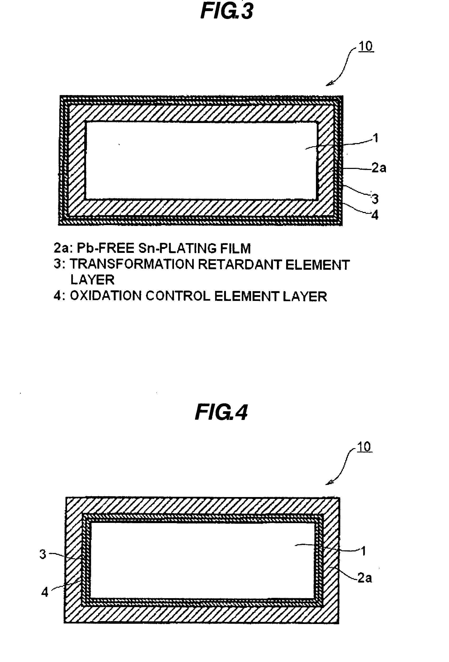
[0063]Sn is used as a base metal of a Sn-plating which is usually used as a plating material of a wiring material. Sn has a two crystal structure types: βSn having a body-centered tetragonal crystal structure (white tin, density of 7.3 g / cm3); and αSn having a diamond type crystal structure (gray tin, density of 5.75 g / cm3). Since an allotropic transformation point where βSn transforms into αSn (hereinafter, referred as “β to α transformation”) is around 13° C. (or less), βSn when manufactured transforms into αSn when used at a temperature not more than the allotropic transformation point. Further, there are two types of Sn oxides each having an oxidation number of 2 and an oxidation number of 4, namely SnO (tin (II) oxide, density of 6.45 g / cm3) which is a black tetragonal crystal, and SnO2 (tin (IV) oxide, density of 6.95 g / cm3) which is a co...
PUM
| Property | Measurement | Unit |
|---|---|---|
| density | aaaaa | aaaaa |
| density | aaaaa | aaaaa |
| density | aaaaa | aaaaa |
Abstract
Description
Claims
Application Information