
In-situ monitoring and method to determine accumulated printed wiring board thermal and/or vibration stress fatigue using a mirrored monitor chip and continuity circuit

a technology of mirrored monitors and continuity circuits, applied in the direction of individual semiconductor device testing, semiconductor/solid-state device testing/measurement, instruments, etc., can solve the problems of increasing the associated life cycle cost, difficult to and complex structure of electronic systems, so as to facilitate the calculation of the total accumulated fatigue experienced, accurately predict the fatigue stress encountered, and the effect of high accuracy of total fatigue estimation

Inactive Publication Date: 2007-12-27
HAMILTON SUNDSTRAND CORP
View PDF24 Cites 17 Cited by
  • Summary
  • Abstract
  • Description
  • Claims
  • Application Information

AI Technical Summary

Benefits of technology

[0013]The large number of solder terminations available by using high density packages such as flip chip and ball grid arrays as monitor chips facilitates calculation of the total accumulated fatigue experienced by any given assembly by using a large sample set of individual terminations. This provides higher levels of accurate total fatigue estimation through large sample sizes than individual accumulated stress types of in-situ sensors. When statistical relationships between monitor chip and functional chip fatigue-to-failure are known, the large number of individual solder terminations available on each monitor chip(s) allow narrow statistical confidence bands to be calculated to accurately predict the fatigue stress encountered to date by the individual assembly on which the monitor chip(s) is(are) mounted based on the number of monitor chip(s) solder terminations and / or locations that have failed to date.

Problems solved by technology

While presently known techniques used to form the terminal and conductor patterns for flip chip and ball grid array packages are generally sufficient, electronic systems are complex structures with characteristics that may make accurate predictive analysis quite difficult.
Predictive analysis, although effective, may not define the risk for all possible failures for individual systems which may result in unnecessary anticipatory preventative maintenance and repair which may increase the associated life cycle costs, or inability to predict imminent failure which can create economic or human costs when failure occurs.

Method used


Image

  • In-situ monitoring and method to determine accumulated printed wiring board thermal and/or vibration stress fatigue using a mirrored monitor chip and continuity circuit
  • In-situ monitoring and method to determine accumulated printed wiring board thermal and/or vibration stress fatigue using a mirrored monitor chip and continuity circuit
  • In-situ monitoring and method to determine accumulated printed wiring board thermal and/or vibration stress fatigue using a mirrored monitor chip and continuity circuit

Examples


Embodiment Construction

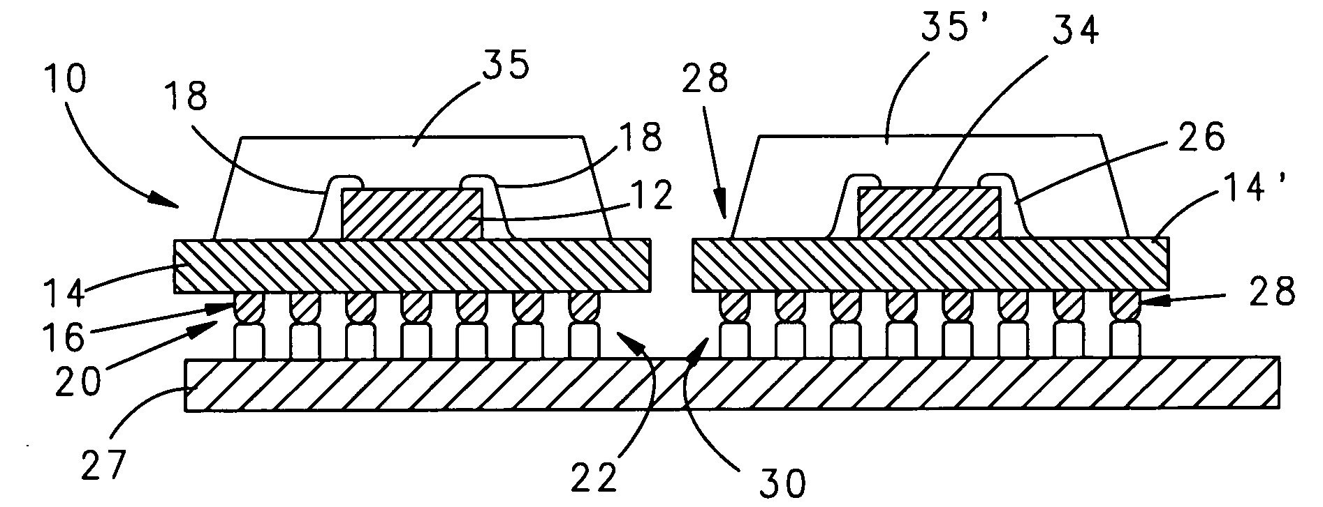
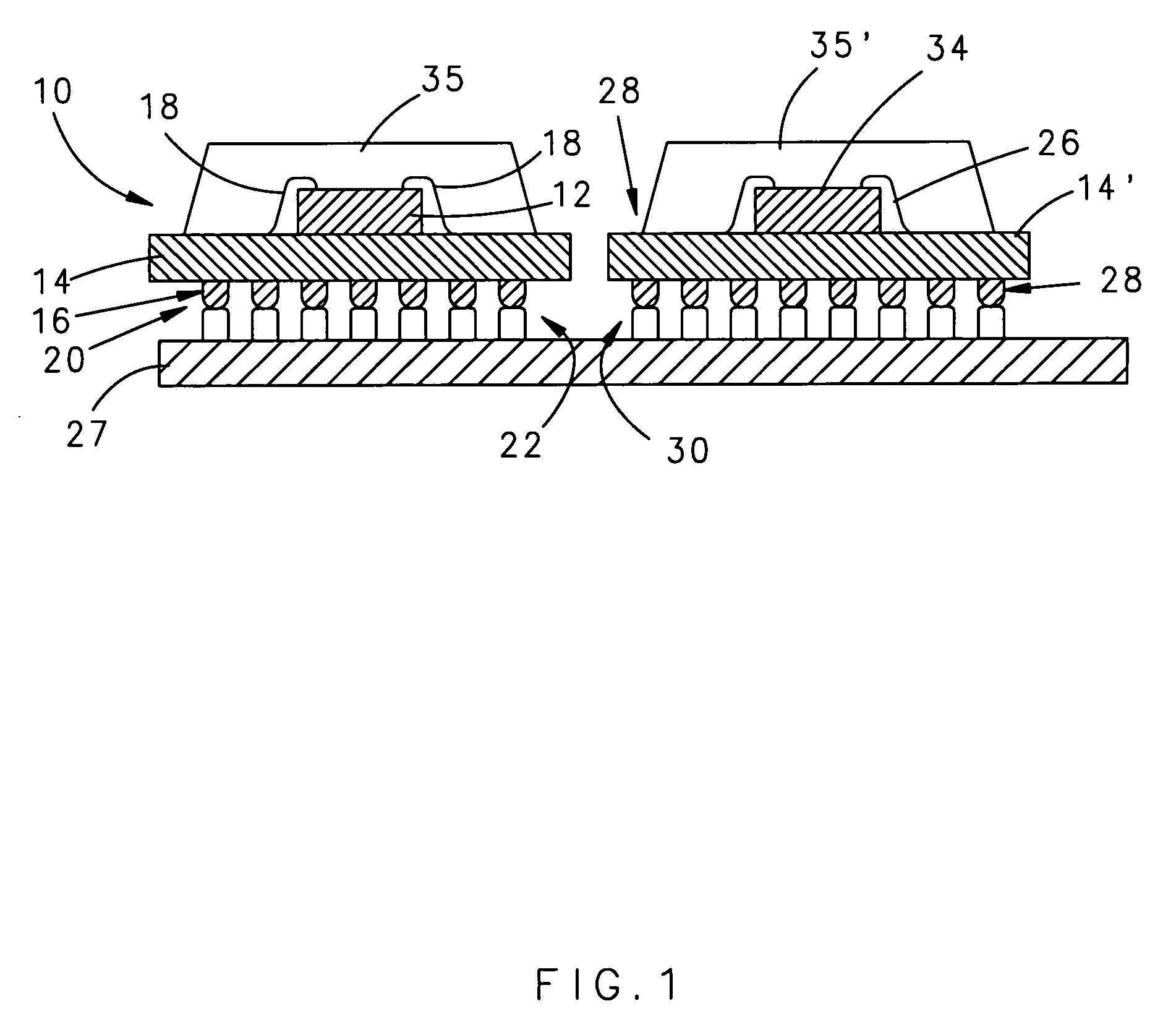
[0020]FIG. 1 illustrates an electronic package 10 having a function IC chip 12 which is wire bonded to a lead frame / package 14 with a number of wires 18. The function IC chip 12 and wires 18 are preferably encapsulated in an encapsulation material 35. The function IC chip 12 as utilized herein may be any semiconductor chip which performs any desired function. Shown here as an example package types are Ball Grid Arrays (BGA). Ball Grid Arrays (BGA) are widely used to electrically and mechanically connect substrate (typically ceramic) carrying semiconductor chips to a card. The BGA attachment method commonly consists of an array of metal pads which are soldered to connecting pads on both the Printed Wiring Board (PWB).

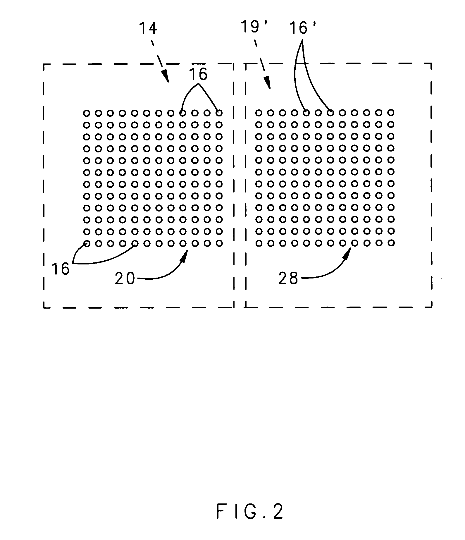
[0021]The wires 18 are routed through the BGA package 14 to terminals, or pads 16, on the opposite surface of the BGA package 14. Similar to the flip-chip process, the pads 16 form a pad pattern 20 (FIG. 2) that serves as interconnects between the integrated circuit chip...


PUM


Abstract

A monitoring system includes a monitor chip or chips soldered to a printed wiring board. By mirroring a function IC chip interface with the monitor chip, the consumed and remaining thermal / and or vibration-fatigue life of the function IC chip based on the life-environment actually experienced through monitoring of the monitor chip is readily determined. The monitor chip includes monitoring interconnections and / or circuitry which determines the number and / or location of failed-open solder terminations of the monitor chip.

Description

BACKGROUND OF THE INVENTION[0001]The present invention relates to determining the accumulated thermal and or vibration fatigue stress fatigue of an electronic system, and more particularly to a mirrored continuity circuit to determine the accumulated printed wiring board fatigue damage.[0002]During its design life, an electronic system can be exposed to a wide variety of vibration and thermal cycling environments. In order to reduce testing time and cost, laboratory tests are usually conducted on products in a time-accelerated manner to create a generalized analytic model that is applied to average or generalized anticipated operating conditions to predict service life of products.[0003]Integrated circuit (IC) chips are often soldered to conductor patterns formed on a circuit board, which may be a ceramic substrate or printed wiring board, in a manner which both secures and electrically interconnects the IC chip to the circuit board. Terminals are formed on the lower surface of the ...

Claims


Application Information

Patent Timeline
IPC IPC(8): H01L23/495
CPCH01L23/3128H05K1/0268H05K3/3436H05K2201/10204H01L2924/15311H05K2203/163H01L2224/48091H05K2201/10734H01L2924/00014
Inventor SCHNETKER, TED R.
Owner HAMILTON SUNDSTRAND CORP
Learn More