Novel way to reduce the ordering temperature for Co2MnSi-like Heusler alloys for CPP, TMR, MRAM, or other spintronics device applications

a technology of co2mnsi and heusler alloy, which is applied in the field of al or feco monolayer insertion in a co2mnsilike heusler layer, can solve the problems of affecting the practical application of gmr or tmr sensors of heusler alloys, affecting the ordering temperature of heusler alloys, and difficult conditions to achieve an ordered half metal structure for co2mnsi/sub>m

Active Publication Date: 2007-12-27
HEADWAY TECH INC
View PDF12 Cites 60 Cited by
  • Summary
  • Abstract
  • Description
  • Claims
  • Application Information

AI Technical Summary

Benefits of technology

[0015]One objective of the present invention is to reduce the ordering temperature of Heusler alloys such as Co2MnS...

Problems solved by technology

However, the condition needed to achieve an ordered half metal structure for Co2MnSi is very difficult and typically requires substrate heating as well as a lengthy high temperature post-annealing treatment.
These post-annealing processes generally require a temperature above 350° C. which would destroy the underlying shield structures (in a TMR head) and severely degrade the pinning strength the...

Method used


Image

  • Novel way to reduce the ordering temperature for Co2MnSi-like Heusler alloys for CPP, TMR, MRAM, or other spintronics device applications
  • Novel way to reduce the ordering temperature for Co2MnSi-like Heusler alloys for CPP, TMR, MRAM, or other spintronics device applications
  • Novel way to reduce the ordering temperature for Co2MnSi-like Heusler alloys for CPP, TMR, MRAM, or other spintronics device applications

Examples


first embodiment

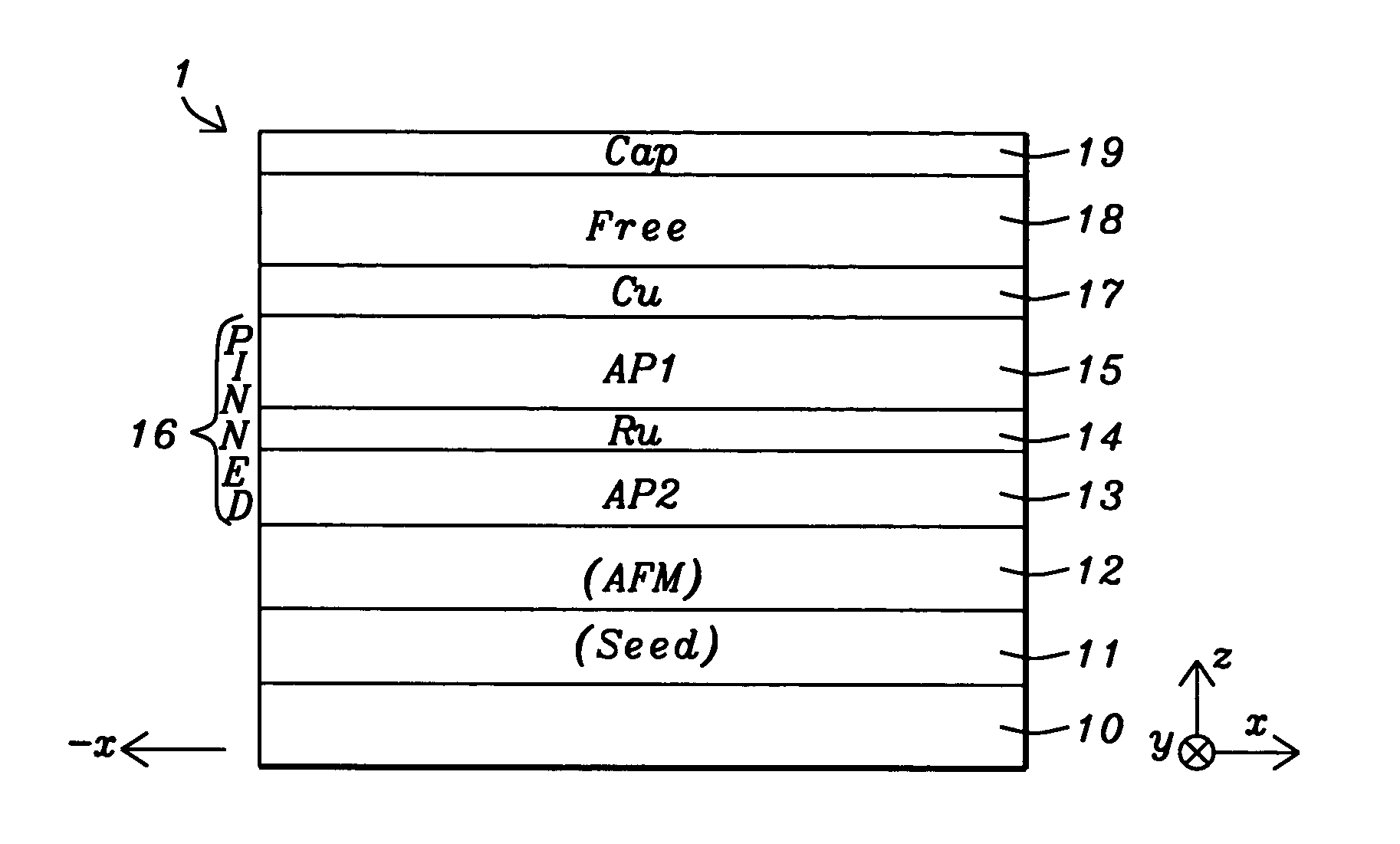
[0027]A first embodiment shown in FIG. 1 relates to a metallic CPP-GMR sensor having a bottom spin valve structure. The view in FIG. 1 is from a cross-section along an air bearing surface (ABS) plane in the read head. A novel spin valve structure 1 will be described first and then a method of forming the stack of layers in the spin valve structure will be provided. Referring to FIG. 1, a substrate 10 is shown that is typically a first magnetic shield (S1) in a read head. For example, the substrate 10 may be comprised of a 2 micron thick layer of an electroplated permalloy. There is a seed layer 11 that may be comprised of a lower Ta layer (not shown) having a thickness from 10 to 60 Angstroms and preferably about 20 Angstroms thick, and an upper Ru layer having a thickness about 5 to 40 Angstroms thick and preferably 20 Angstroms thick formed on the substrate 10. The seed layer 11 promotes a smooth and uniform crystal structure in the overlying layers that enhances the MR ratio in t...

second embodiment

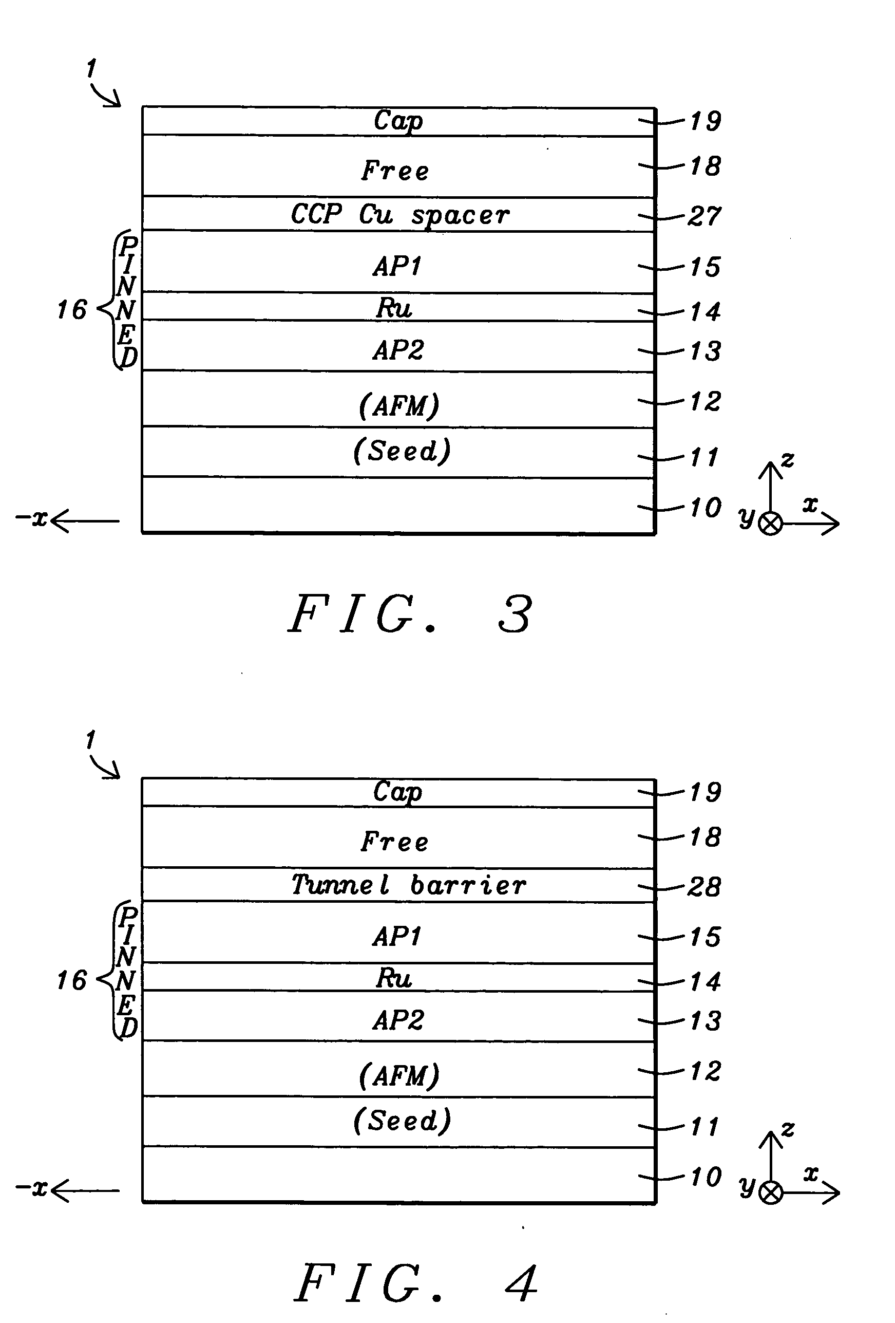
[0036]In a second embodiment depicted in FIG. 3 that relates to a CCP CPP-GMR sensor, the spin valve structure is similar to that previously described except the spacer 17 is replaced by a composite spacer layer 27 comprised of a confining current path (CCP) layer (not shown) formed between lower and upper copper layers (not shown). As mentioned previously, a CCP layer may be employed in a spin valve structure to improve performance. In one aspect, the lower Cu layer is about 2 to 8 Angstroms thick and preferably 5.2 Angstroms thick, and the upper Cu layer has a thickness between 2 and 6 Angstroms and is preferably 3 Angstroms thick. The CCP layer may be made of AlCu that has been partially oxidized by a process described in a later section. The CCP layer has a thickness from 6 to 10 Angstroms and is preferably a AlCu layer having a thickness of about 8.5 Angstroms and an Al content of about 90 atomic %. The Cu / AlCu / Cu composite spacer layer 27 may be further modified by inserting a...


PUM


Abstract

A spin valve structure is disclosed in which an AP1 layer and/or free layer are made of a laminated Heusler alloy having Al or FeCo insertion layers. The ordering temperature of a Heusler alloy such as Co2MnSi is thereby lowered from about 350° C. to 280° C. which becomes practical for spintronics device applications. The insertion layer is 0.5 to 5 Angstroms thick and may also be Sn, Ge, Ga, Sb, or Cr. The AP1 layer or free layer can contain one or two additional FeCo layers to give a configuration represented by FeCo/[HA/IL]nHA, [HA/IL]nHA/FeCo, or FeCo/[HA/IL]nHA/FeCo where n is an integer≧1, HA is a Heusler alloy layer, and IL is an insertion layer. Optionally, a Heusler alloy insertion scheme is possible by doping Al or FeCo in the HA layer. For example, Co2MnSi may be co-sputtered with an Al or FeCo target or with a Co2MnAl or Co2FeSi target.

Description

RELATED PATENT APPLICATIONS[0001]This application is related to the following: Docket# HT03-009, Ser. No. 10 / 796,387, filing date Mar. 9, 2004; Docket# HT03-043, Ser. No. 10 / 886,288, filing date Jul. 7, 2004; Docket# HT05-015, Ser. No. 11 / 180,808, filing date Jul. 13, 2005; and Docket# HT05-042 / 053, Ser. No. 11 / 352,676, filing date Feb. 13, 2006, all assigned to a common assignee.FIELD OF THE INVENTION[0002]The invention relates to Al or FeCo monolayer insertions in a Co2MnSi-like Heusler layer that serves as a free layer or AP1 pinned layer in a giant magnetoresistive (GMR) sensor having a current perpendicular to plane (CPP) configuration, or in a tunneling magnetoresistive (TMR) read head or magnetoresistive random access memory (MRAM) device.BACKGROUND OF THE INVENTION[0003]A CPP-GMR head is considered as one promising sensor to replace the conventional CIP (current in plane) GMR head for over 100 Gb / in2 recording density. In a typical CPP-GMR sensor, a bottom synthetic spin val...

Claims


Application Information

Patent Timeline
IPC IPC(8): G11B5/127
CPCB82Y10/00H01F10/3259G01R33/093G11B5/3906G11B5/3909G11B5/3983G11C11/16H01F10/1936H01F10/3254H01F10/3272H01F41/183H01L43/08H01L43/10H01L43/12H01F10/3295B82Y25/00H10N50/01H10N50/85H10N50/10
Inventor ZHANG, KUNLIANGLI, MINCHEN, YU-HSIAWANG, HUI-CHUANZHAO, TONG
Owner HEADWAY TECH INC
Why Eureka
Try Eureka