Semiconductor optical device and optical transmission module

a technology of semiconductor optical devices and optical transmission modules, which is applied in the direction of semiconductor lasers, nanotechnology, lasers, etc., can solve the problems of difficult mass-production of semiconductor optical devices, difficult to stably provide materials, adversely affecting the modulation band of ea modulators, etc., to facilitate the design of capacitors, reduce time and cost, and reduce the condition of crystal growth

Active Publication Date: 2007-12-27
LUMENTUM JAPAN INC
View PDF3 Cites 17 Cited by
  • Summary
  • Abstract
  • Description
  • Claims
  • Application Information

AI Technical Summary

Benefits of technology

[0032] The invention can be used to fabricate an optical device that integrates a laser portion with an excellent characteristic for DWDM optical transmission, and a low-capacitance modulator portion which facilitates the design of the capacitor. The invention can provide a high-yield semiconductor optical device regardless of the base material for forming the active layer for forming the semiconductor optical device. Even in a modulator integrated laser including an InGaAsP-based MQW, the

Problems solved by technology

Therefore, the diffused Zn undesirably produces an uncontrollable parasitic capacitance or causes a sudden increase in capacitance in the mesa side, thereby adversely affecting the modulation band of the EA modulator.
While the use of Ru has such an advantage as to make the capacitance of the EA modulator portion easily controllable, since Ru is hardly interdiffused with Zn, it is difficult to stably provide the material.
It is therefore difficult to mass-produce s

Method used


Image

  • Semiconductor optical device and optical transmission module
  • Semiconductor optical device and optical transmission module
  • Semiconductor optical device and optical transmission module

Examples


first embodiment

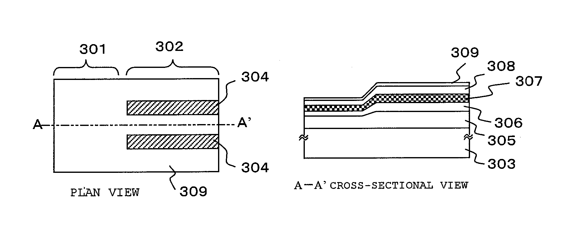
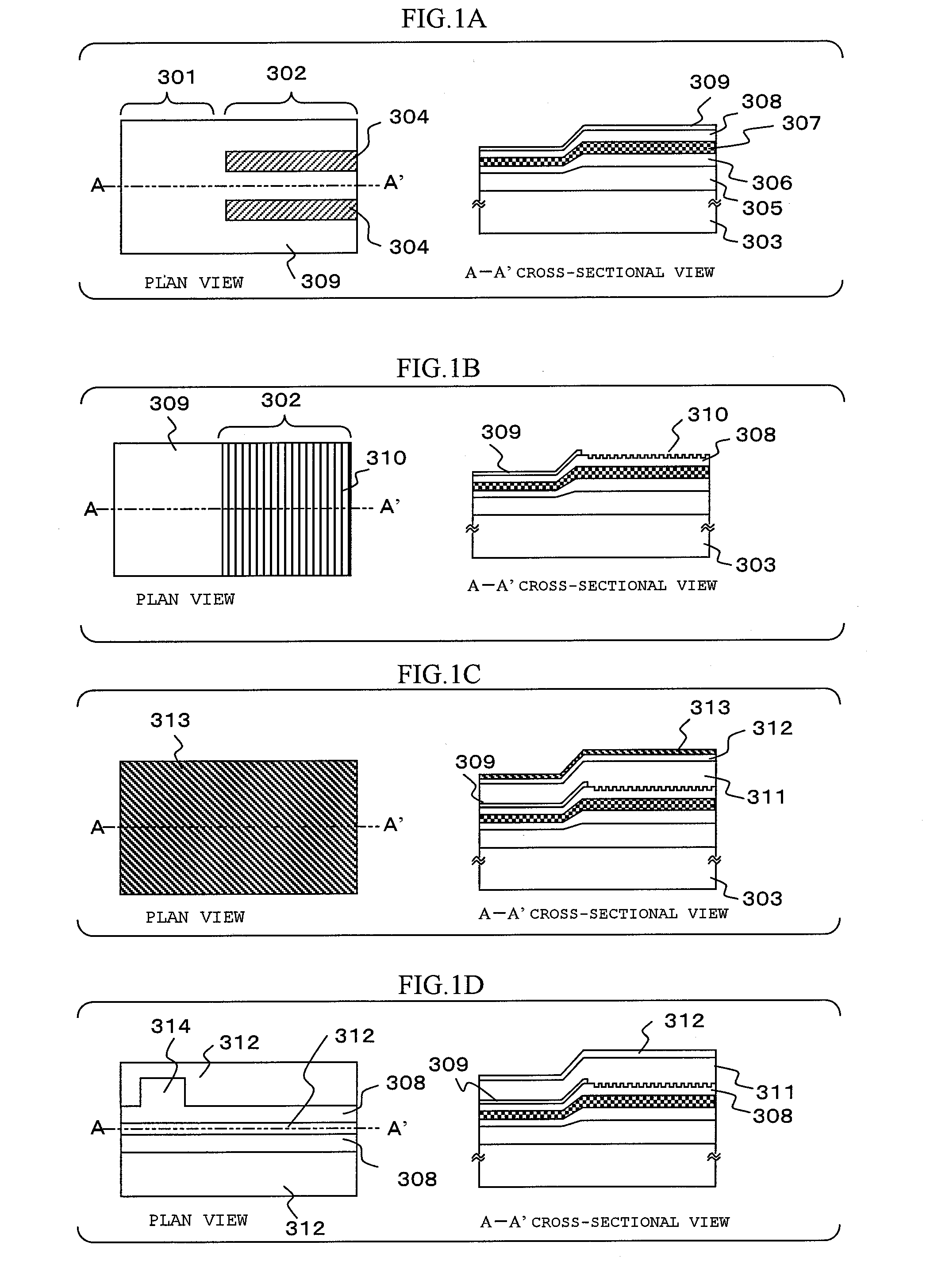
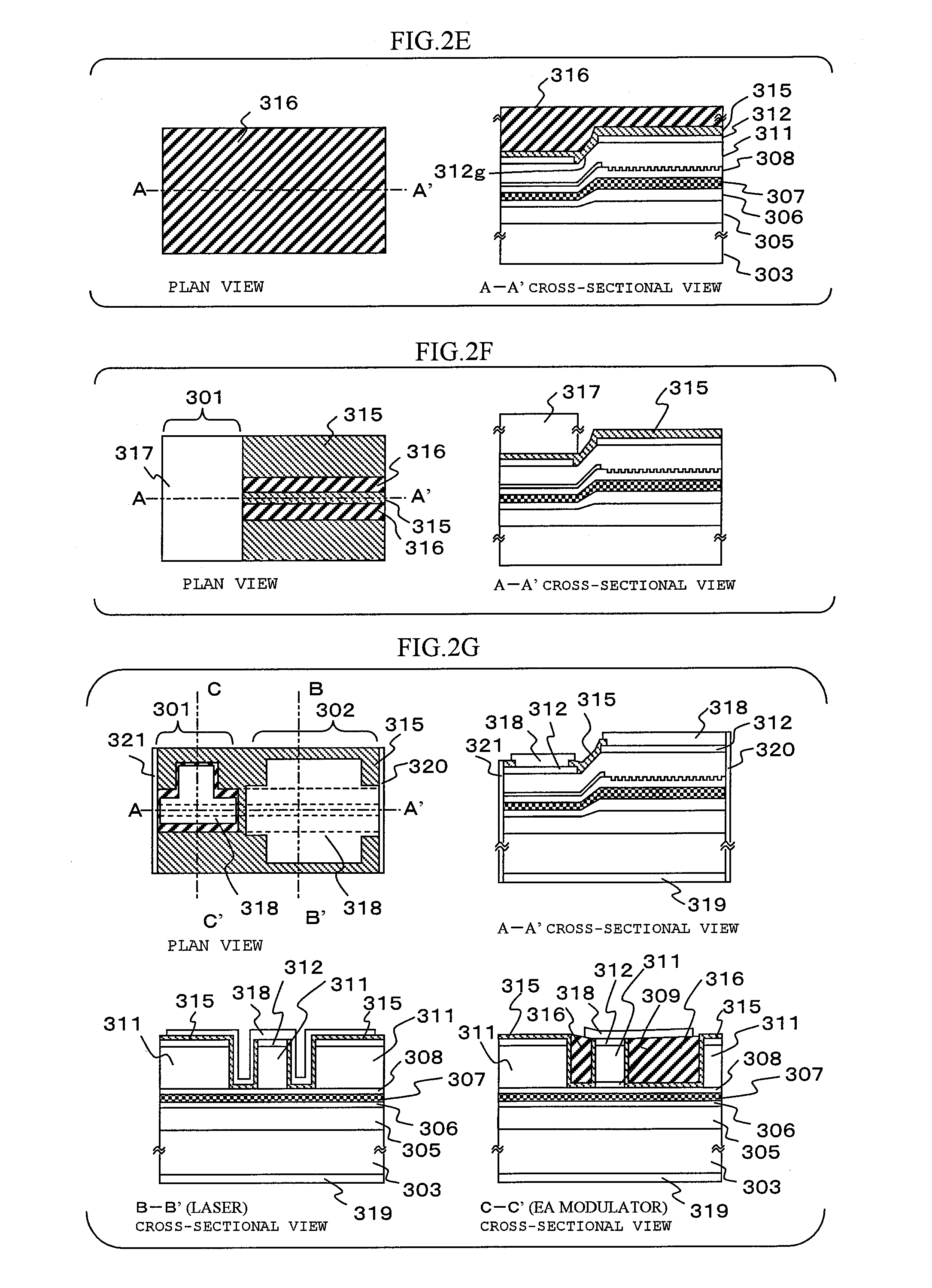
[0040] A first embodiment of the invention will be described. Referring to FIGS. 1A to 1D and FIGS. 2E to 2G, a description will be given below of a method of fabricating an EA / DFB integrated laser in which an EA modulator portion 301 takes a polyimide-resin-buried ridge waveguide structure and a laser portion 302 takes a ridge waveguide structure having air around a mesa. FIGS. 1A to 1D and FIGS. 2E to 2G each show a plan view and a cross-sectional view.

[0041] First, SiO2 films 304 are formed on an n-type semiconductor substrate 303 by T-CVD, and the SiO2 films 304 sandwiching that region of a laser portion 302 equivalent to a mesa are patterned. With the SiO2 films 304 as masks, an n-type InP buffer layer 104, an n-type InGaAsP lower guide layer 306, an MQW 307 having a well / barrier layer of InGaAsP, a p-type InGaAsP upper guide layer 308, and a p-type InP cap layer 309 are grown in order by selective growth called MO-CVD (first multilayer growth: FIG. 1A)

[0042] Thereafter, the ...

second embodiment

[0057]FIGS. 3A to 3C are diagrams for explaining a second embodiment of the invention. FIG. 3A is a plan view, FIG. 3B is a cross-sectional view along A-A′, and FIG. 3C is a cross-sectional view along B-B′.

[0058] The following description of the embodiment will be given of a case where an external modulator is a Mach-Zehnder modulator. Specifically, the embodiment is a semiconductor optical device which has the integration of a Mach-Zehnder modulator portion 401 having a polyimide-resin buried ridge waveguide structure, and a laser portion 402 having a ridge waveguide structure having air around the mesa.

[0059] This device can be fabricated through substantially the same processes as described in the foregoing description of the first embodiment. First, an n-type InP buffer layer 404, an n-type InGaAsP lower guide layer 405, an MQW 406 of InGaAsP, a p-type InGaAsP upper guide layer 407, and a p-type InP cap layer 408 are grown on an n-type InP substrate 403 in the first multilayer...

third embodiment

[0062]FIGS. 4A to 4C are diagrams for explaining a third embodiment of the invention. FIG. 4A is a plan view, FIG. 4B is a cross-sectional view along A-A′, and FIG. 4C is a cross-sectional view along B-B′.

[0063] The following description of the embodiment will be given of an EA / DFB integrated laser with a ridge waveguide structure which uses InGaAlAs for an MQW.

[0064] A feature of InGaAlAs lies in the fact that the band offset ΔEv of the valence-band is smaller and the band offset ΔEc of the conduction-band is larger than those of InGaAsP. That is, the use of InGaAlAs in the laser portion ensures sufficiently strong electron confinement and uniform hole injection, so that electrons do not easily leak from the MQW even at a high temperature, thus making it possible to ensure a stable operation over a wide temperature range.

[0065] The use of InGaAlAs in the EA modulator portion can sufficiently confine electrons even if confinement of holes is made weaker to improve the chirp chara...


PUM


Abstract

A semiconductor optical device has a semiconductor laser portion and a modulator portion which have different mesa structures. The mesa structure of the semiconductor laser portion is a ridge waveguide structure which has air around the mesa. The mesa structure of the modulator portion is a planarized ridge waveguide structure which has an organic insulator buried around the mesa.

Description

[0001] The present invention relates generally to a semiconductor optical device, and more particularly, to an external modulator integrated laser which operates at a transmission rate of 2.5 Gbits / s or higher, and an optical transmission module having the external modulator integrated laser mounted thereon. [0002] At present, dense wavelength division multiplexing (DWDM) optical transmission which transmits optical signals of multiple wavelengths in a single optical fiber most typically uses a transmission system which enables long-range transmission at a transmission rate of 2.5 Gbits / s or higher, and in particular, 10 Gbits / s. Market demand for a transmission rate of 40 Gbits / s has recently been gradually increasing. [0003] In the DWDM optical transmission, a grid wavelength with a wavelength band of 1.55 μm that realizes long-range optical transmission is defined in the ITU-T standards. The wavelength interval (frequency interval) of the grid wavelength is 0.4 nm (50 GHz) or 0.8...

Claims


Application Information

Patent Timeline
IPC IPC(8): H01S5/20
CPCB82Y20/00H01S5/02248H01S5/02284H01S5/026H01S5/0265H01S5/34306H01S5/0425H01S5/0683H01S5/22H01S5/2213H01S5/0287H01S5/04254H01S5/04256H01S5/02251H01S5/02325
Inventor SASADA, NORIKONAOE, KAZUHIKO
Owner LUMENTUM JAPAN INC
Why Eureka
Try Eureka