
Method of fabricating semiconductor device and semiconductor device

a semiconductor and semiconductor technology, applied in the field of semiconductor devices, can solve the problems of difficult to increase the impurity concentration at the interface between silicide film b, physicality limits, and the inability to achieve higher performance by nano-scale miniaturization of on-chip devices, and achieve the effect of preventing or suppressing the occurrence of junction leakage, low resistance junction interfaces, and reducing the number of junction leakages

Inactive Publication Date: 2007-12-27
KK TOSHIBA
View PDF2 Cites 35 Cited by
  • Summary
  • Abstract
  • Description
  • Claims
  • Application Information

AI Technical Summary

Benefits of technology

[0010]The present invention was made in view of the above-noted background, and its object is to provide a semiconductor device having high-performance MISFETs with low resistance junction interface while reducing junction leakage and also a fabrication method of the semiconductor device.
[0017]In accordance with the invention as disclosed herein, it becomes possible to provide a semiconductor device having high-performance MISFETs with low resistance junction interfaces while preventing or at least greatly suppressing the occurrence of junction leakage, and also provide a fabrication method of the semiconductor device.

Problems solved by technology

Until today, the device performance enhancement has been principally achieved based on proportional downsizing rules, called the “scaling.” However, in recent years, not only challenges to achieve higher performance by nanoscale miniaturization of on-chip devices but also chip designs for retaining operability of these devices per se are facing up to difficult circumstances.
This is largely due to the presence of various limits in physical properties.
One of such physicality limits is a problem as to parasitic resistance components in source / drain (S / D) regions.
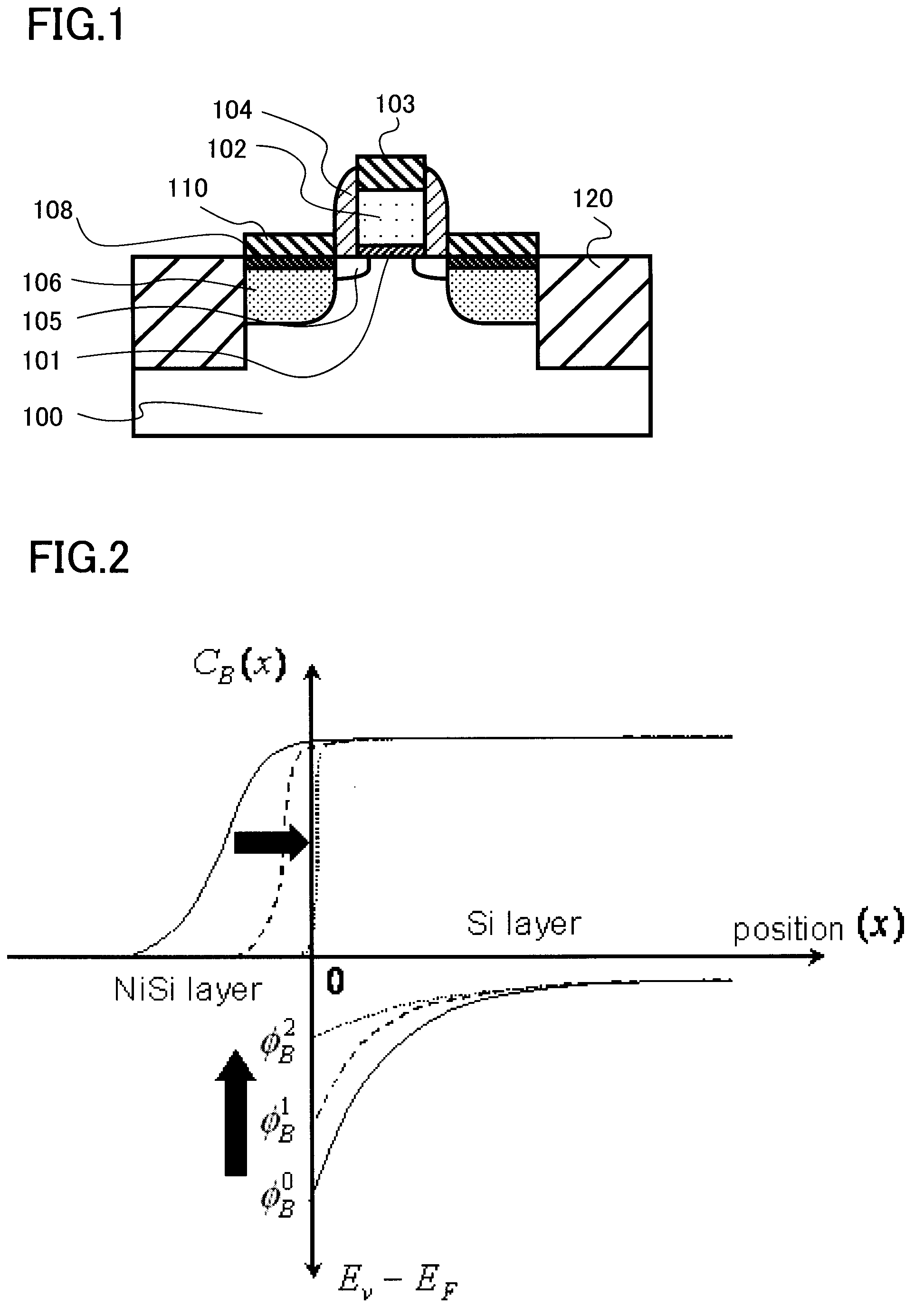
With this process, however, it has been difficult to increase the impurity concentration at the interface between silicide film 110 and heavily-doped impurity region 107—in particular, in the case of p-type silicon (Si).
As apparent from the foregoing, the prior art NiSi layer formation process is faced with a problem as to the difficulty in lowering the junction interface resistance Rc.
It is also known that the use of NiSi film for S / D electrodes can result in an unwanted increase in junction leakage current due to the fact that Ni atoms readily diffuse in silicon.

Method used


Image

  • Method of fabricating semiconductor device and semiconductor device
  • Method of fabricating semiconductor device and semiconductor device
  • Method of fabricating semiconductor device and semiconductor device

Examples


first embodiment

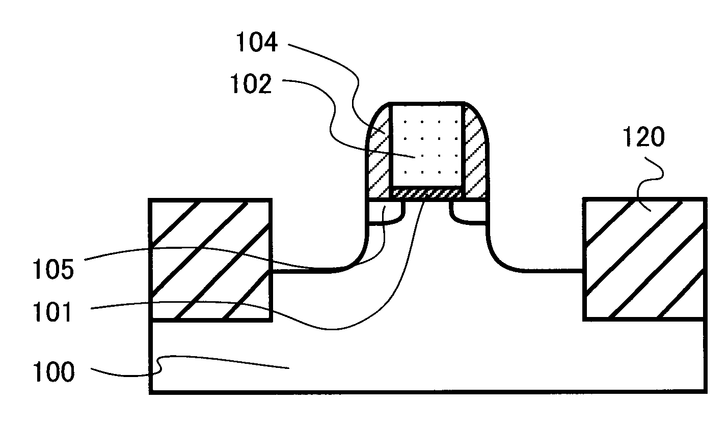
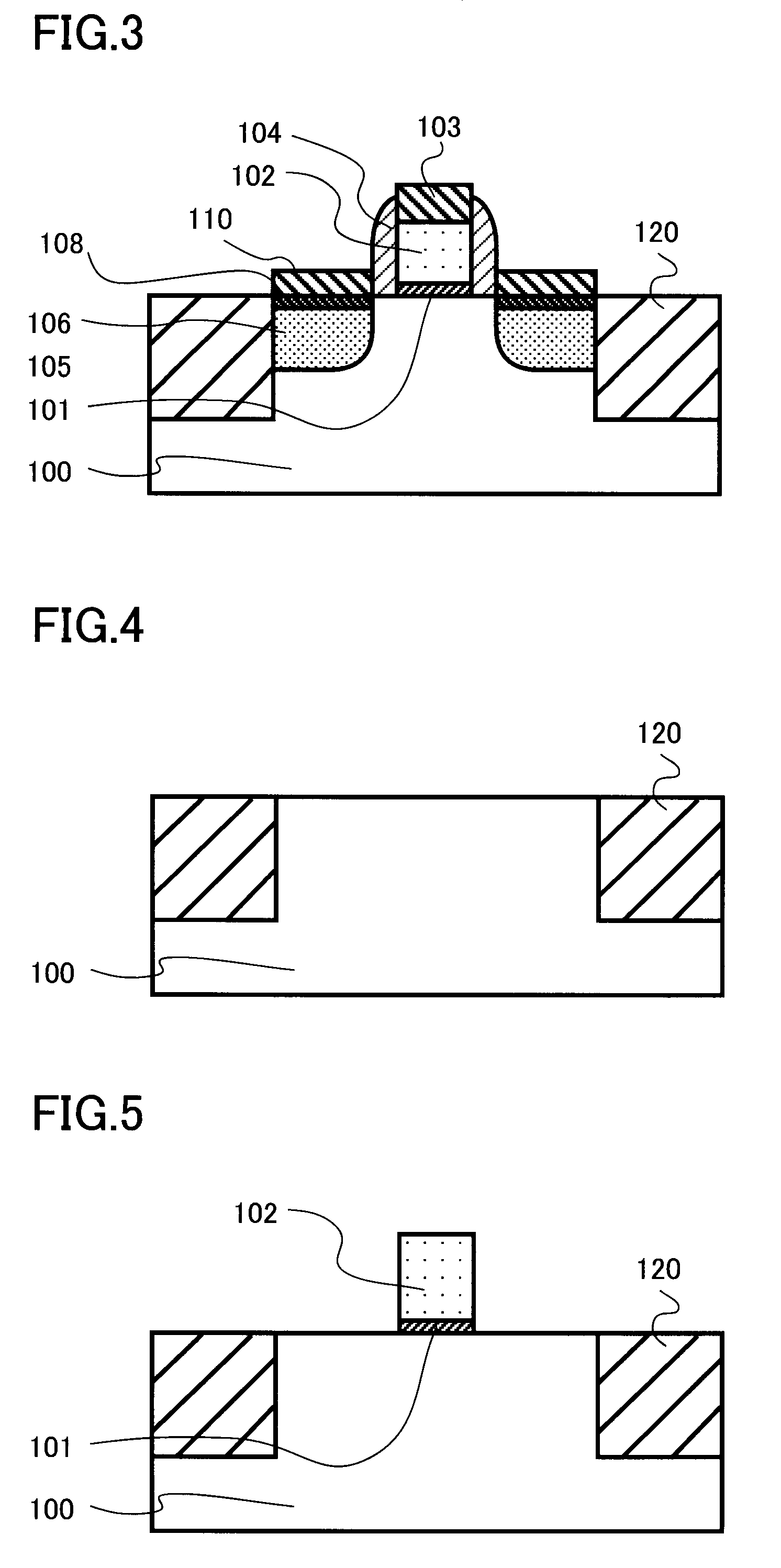
[0049]A semiconductor device having a metal insulator semiconductor field effect transistor (MISFET) in accordance with an embodiment of this invention is depicted in cross-section in FIG. 1. The MISFET is illustratively a p-conductivity type MISFET (pMISFET), which has a pair of laterally spaced-apart portions of a SiGe layer on the both sides of a channel region and a nickel silicide (NiSi) layer that is formed above SiGe layer with a heavily-doped impurity region interposed therebetween. In the description, the term first conductivity type refers to either one of n-type and p-type whereas the term second conductivity type is the other of them. The first and second conductivity types are different from each other.

[0050]More specifically, a silicon (Si) substrate (first semiconductor region as claimed) 100 of n-type conductivity has a top surface of a (100) surface orientation, which is doped with a chosen impurity, e.g., phosphorus (P), to a concentration of about 1015 atoms / cm3. ...

second embodiment

[0081]A semiconductor device structure having a MISFET in accordance with another embodiment of this invention is shown in FIG. 14 in cross-section. This device is similar to the pFET shown in FIG. 1 except that the former has a fully silicided (FUSI) structure with its gate electrode being formed of NiSi gate silicide layer 103 only.

[0082]This semiconductor device of FIG. 2 offers the functionality and advantages stated previously and also is capable of suppressing depletion on the gate electrode side during transistor driving within an extended range up to a higher gate voltage owing to the use of FUSI structure to thereby enable achievement of enhanced transistor drivability.

[0083]A fabrication method of the FIG. 14 device is similar to the method shown in FIGS. 4 to 13 except that the step of FIG. 12 for sputtering the Ni film 150 and performing silicidation by annealing is modified to perform the annealing for an increased length of time period until the polysilicon gate electr...

third embodiment

[0087]A semiconductor device having a MISFET to be formed by a fabrication method in accordance with still another embodiment of the invention is shown in FIG. 15 in cross-section. This device has an nFET of FUSI structure with its gate electrode being made up of only a silicide monolayer 103 made of NiSi and a pair of NiSi S / D electrodes 110. The device also has at selected substrate surface portions a couple of heavily-doped n (n+) type impurity regions 208, each being doped with As and C impurities to a concentration of 1021 atoms / cm3 or greater but less than or equal to 1022 atoms / cm3. The presence of these n+-type S / D regions 208 is a unique structural feature of this embodiment.

[0088]A feature of this nFET lies in that the NiSi layer is high in impurity concentration at its substrate interface due to the presence of the n+-type S / D regions 208 so that the interface resistance is low. Another feature is that n+-type regions 208 serve as the barrier against unwanted diffusion of...


PUM


Abstract

A semiconductor device includes a first semiconductor region of first type conductivity with a channel region being formed therein, a gate electrode insulatively formed above the channel region, a layer of SixGe1-x (0<x<1) on both sides of the channel region, a pair of second semiconductor regions of second type conductivity as formed on the SixGe1-x layer to have a controlled impurity concentration ranging from 1021 to 1022 atoms / cm3, and a nickel-containing silicide layer above the second semiconductor regions. A fabrication method of the semiconductor device is also disclosed.

Description

CROSS-REFERENCE TO RELATED APPLICATION[0001]This application is based on and claims priority of Japanese Patent Application (JPA) No. 2006-173062, filed Jun. 22, 2006, the disclosure of which is incorporated herein by reference.FIELD OF THE INVENTION[0002]The present invention relates generally to semiconductor devices, and more particularly to a semiconductor device having a metal insulator semiconductor field effect transistor (MISFET) with improved source / drain (S / D) structure. This invention also relates to a method of fabricating the semiconductor device.BACKGROUND OF THE INVENTION[0003]Silicon-based ultralarge-scale integrated (ULSI) circuit is one of key technologies that support highly advanced information-intensive societies in near future. For further advances in functionality of silicon ULSI devices, it is inevitable to enhance the performance of MISFETs for use as major circuit elements on ULSI chips. Until today, the device performance enhancement has been principally a...

Claims


Application Information

Patent Timeline
Patent Type & Authority Applications(United States)
IPC IPC(8): H01L21/8234H01L21/336
CPCH01L21/26513H01L21/28097H01L21/823814H01L29/66636H01L29/665H01L29/6659H01L29/66628H01L21/823835
Inventor YAMAUCHI, TAKASHIKINOSHITA, ATSUHIROTSUCHIYA, YOSHINORIKOGA, JUNJI
Owner KK TOSHIBA
Learn More