

Low-temperature doping processes for silicon wafer devices
a technology of silicon wafers and low-temperature doping, which is applied in the direction of photovoltaic energy generation, crystal growth processes, electrical equipment, etc., can solve the problems of requiring ultra-thin intrinsic buffer layers and complex current low-temperature si cell fabrication processes, and achieve the effects of increasing the concentration of crystal defects, increasing the thickness of the doped silicon layer, and increasing the quality of the doped layer
- Summary
- Abstract
- Description
- Claims
- Application Information
AI Technical Summary
Benefits of technology
Problems solved by technology
Method used
Image

Examples
Embodiment Construction
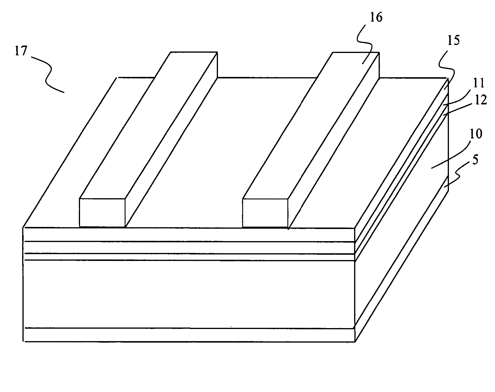
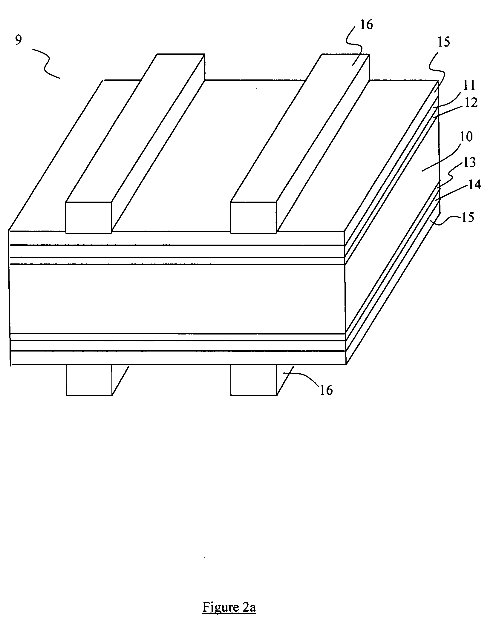
[0040] A Low Temperature (LT) fabrication scheme 200 (see FIG. 15) for silicon wafer devices 21 (see FIG. 14) is described, with the resulting crystal structure of the devices 21 including a silicon substrate 22 attached to a grown thin film layer 23 (silicon based), thereby defining an interface 114. It is recognized that the fabrication scheme can be used for manufacturing a number of different silicon wafer devices 21 for differing technology applications, such as but not limited to photovoltaic cells used in manufacturing of solar systems for the conversion of sunlight into electrical energy. It is recognized that the fabrication scheme 200, and resultant silicon wafer device 21 structure, are different from other High Temperature (HT) and other LT fabrication schemes and their corresponding silicon wafer devices 1, 9, 17 (see FIGS. 1, 2a, 2b).
Solar Cell Examples
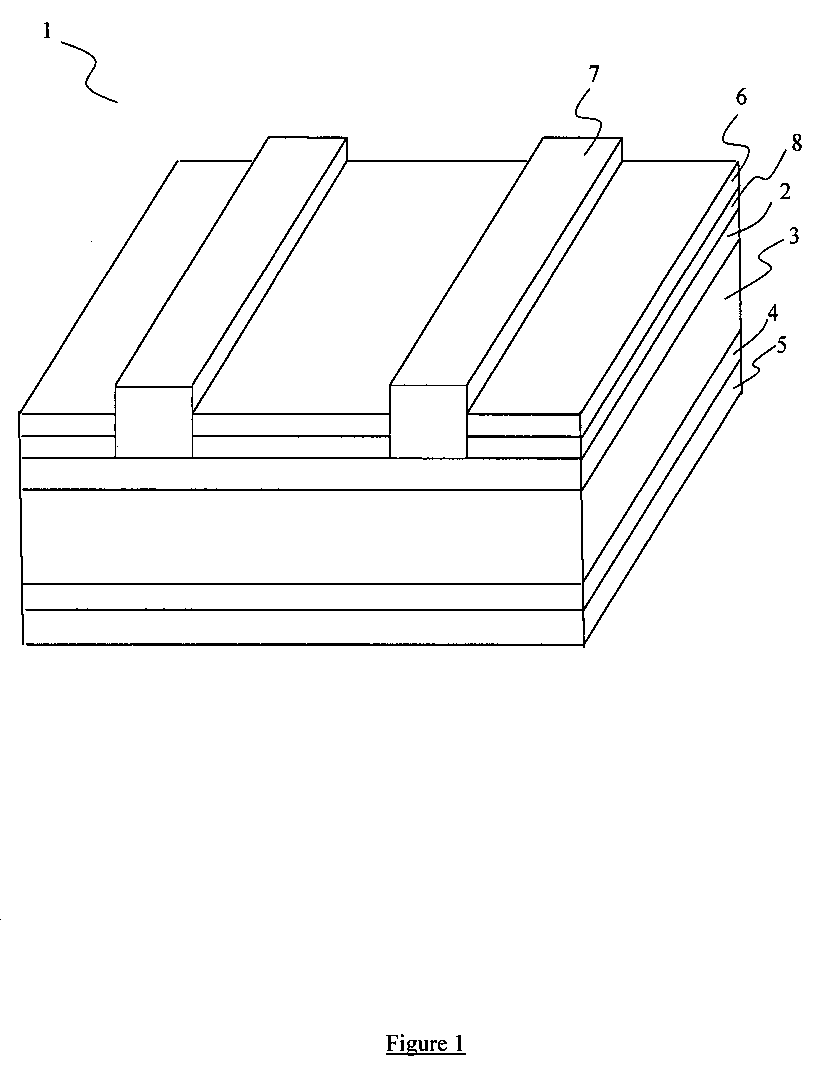
[0041] Referring to FIG. 1, shown is an example wafer structure of a HT processed conventional n+pp+ silicon solar ...
PUM
| Property | Measurement | Unit |
|---|---|---|
| thickness | aaaaa | aaaaa |
| temperature | aaaaa | aaaaa |
| temperature | aaaaa | aaaaa |
Abstract
Description
Claims
Application Information