

Semiconductor device and method of manufacturing the same
a technology of semiconductor devices and semiconductors, applied in the direction of semiconductor devices, basic electric elements, electrical equipment, etc., can solve the problems of reducing the separation distance cannot be reduced, so as to improve reduce the resistance value of the back gate region, and improve the effect of the breakdown voltage characteristic of the mos transistor
- Summary
- Abstract
- Description
- Claims
- Application Information
AI Technical Summary
Benefits of technology
Problems solved by technology
Method used
Image

Examples
Embodiment Construction
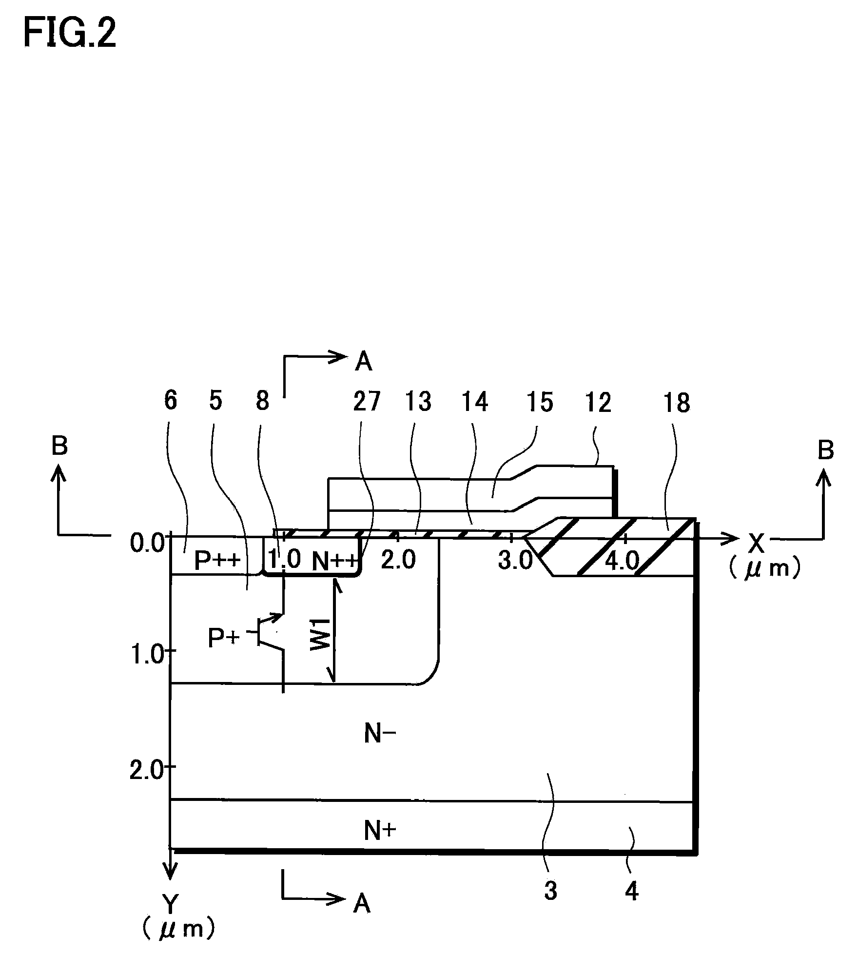
[0025]Hereinafter, descriptions will be given in detail of a semiconductor device according to a preferred embodiment of the present invention with reference to FIGS. 1 to 3. FIG. 1 is a cross-sectional view for describing the semiconductor device according to this preferred embodiment. FIG. 2 is a cross-sectional view for describing the semiconductor device according to this preferred embodiment. FIG. 3 shows impurity concentration profiles for describing the semiconductor device according to this preferred embodiment.
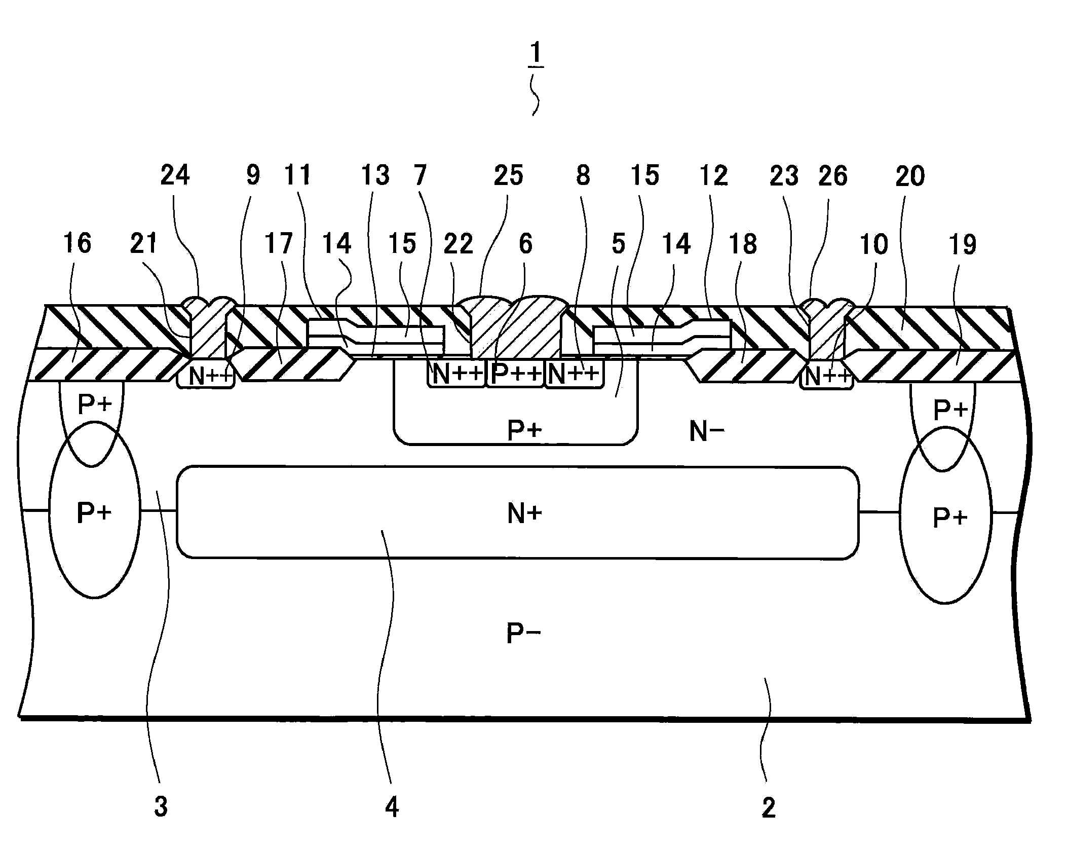
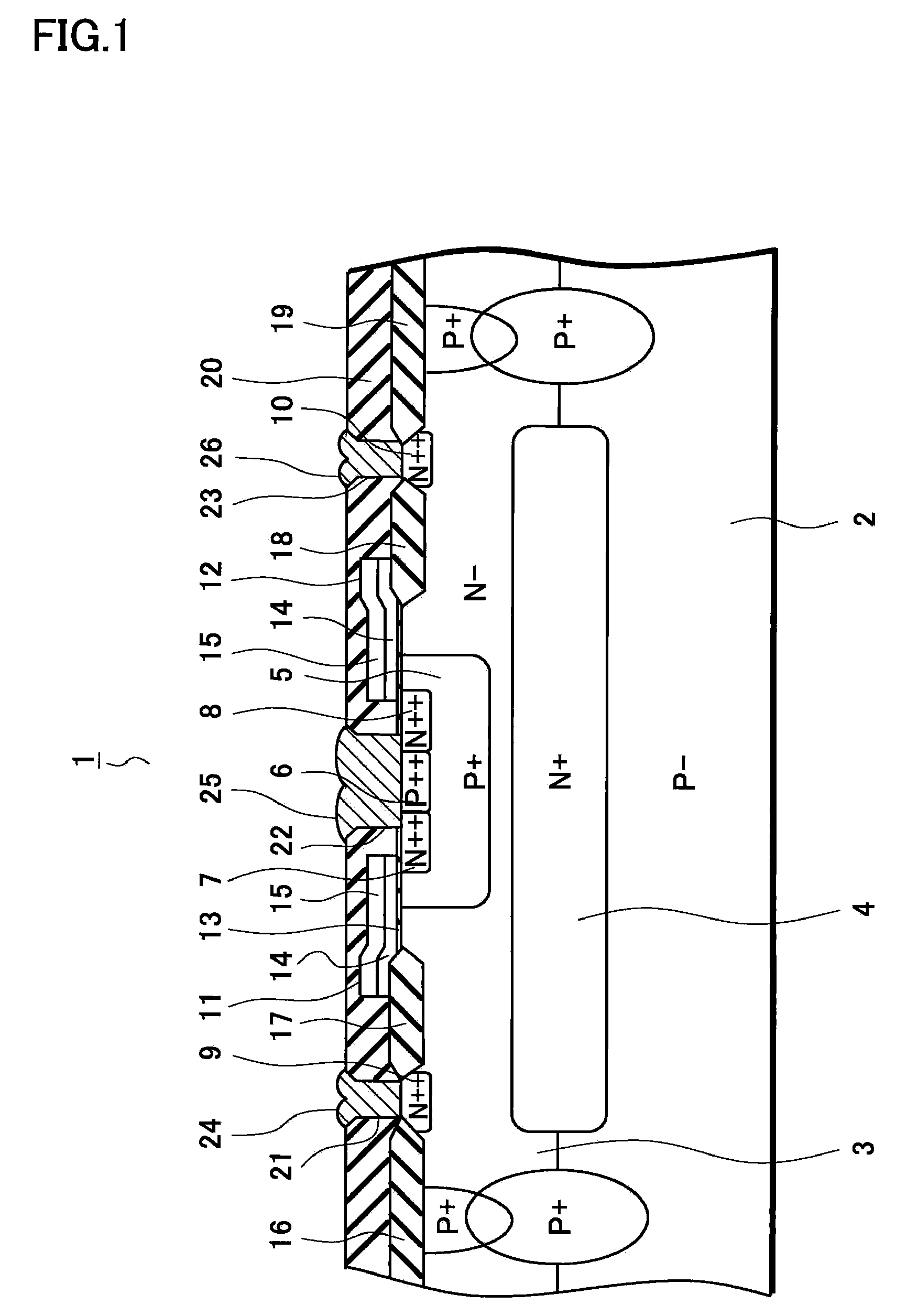
[0026]As shown in FIG. 1, an N-channel MOS transistor 1 mainly includes a P type single crystal silicon substrate 2, an N type epitaxial layer 3, an N type buried diffusion layer 4, P type diffusion layers 5 and 6, which are used as back gate regions, N type diffusion layers 7 and 8, which are used as source regions, N type diffusion layers 9 and 10, which are used as drain regions, and gate electrodes 11 and 12.
[0027]The N type epitaxial layer 3 is formed on the P ty...
PUM
 Abstract
Description
Claims
Application Information