

Return-to-hold switching scheme for dac output stage
a switching scheme and output stage technology, applied in the field of mixed signal converters, can solve the problems of inter-symbol interference (isi), un-equal rise and fall time in waveform, and ac distortion equal to high-power dacs with dissipation as much as 10 times larger, so as to and eliminate inter-symbol interference error
- Summary
- Abstract
- Description
- Claims
- Application Information
AI Technical Summary
Benefits of technology
Problems solved by technology
Method used
Image

Examples
Embodiment Construction
[0026]While this invention is illustrated and described in a preferred embodiment, the invention may be produced in many different configurations. There is depicted in the drawings, and will herein be described in detail, a preferred embodiment of the invention, with the understanding that the present disclosure is to be considered as an exemplification of the principles of the invention and the associated functional specifications for its construction and is not intended to limit the invention to the embodiment illustrated. Those skilled in the art will envision many other possible variations within the scope of the present invention.
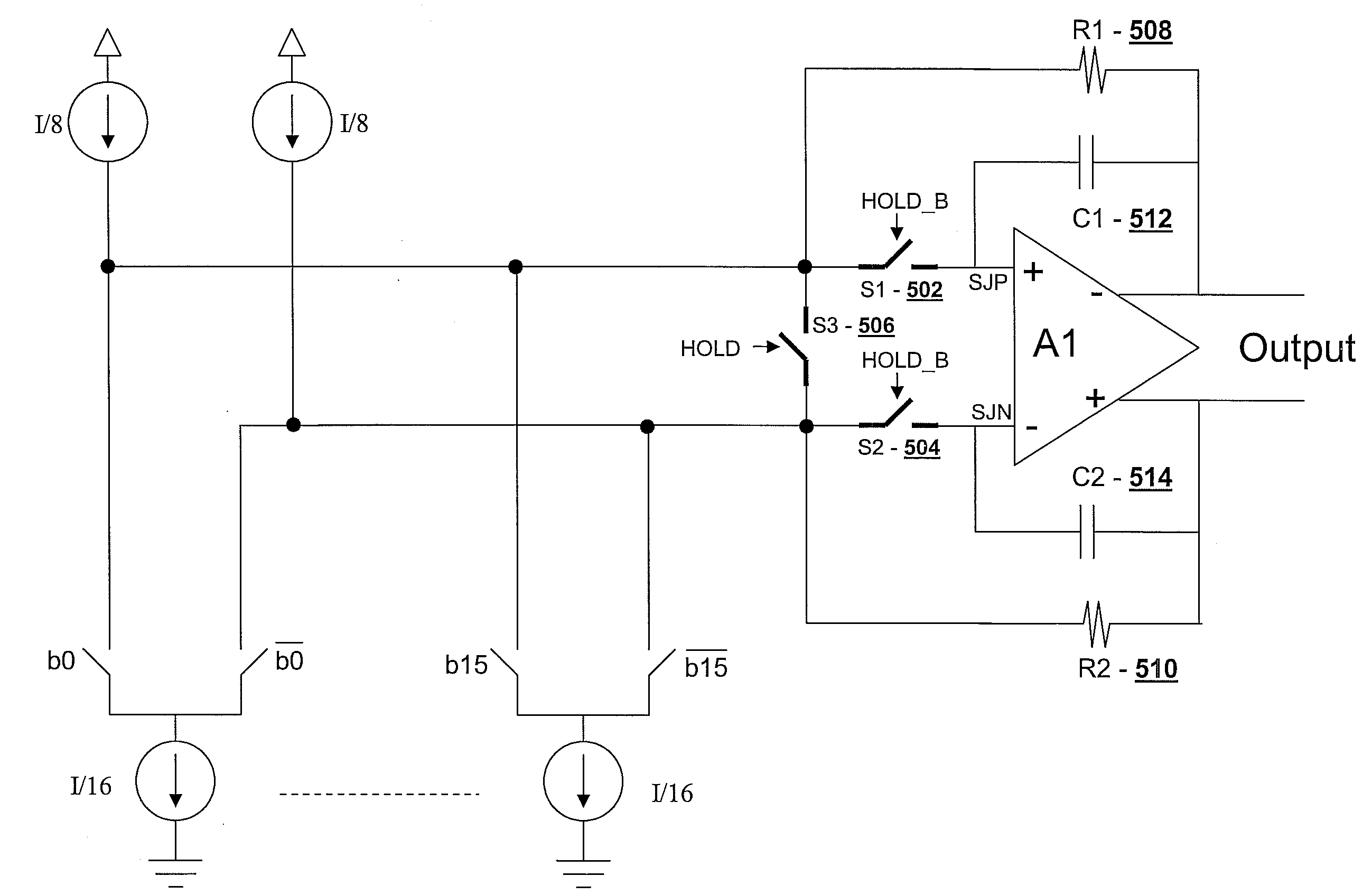
[0027]FIG. 5 illustrates a block diagram of the present invention's return-to-hold scheme wherein the current steering DAC output stage with the addition of switches S1502, S2504, and S3506. Switches S1502 and S2504 are controlled by a HOLD_B signal while switch S3506 is controlled by a HOLD signal. The timing diagram of the clock, the current cell con...
PUM
 Abstract
Description
Claims
Application Information