

Material processing method for semiconductor lasers
a semiconductor laser and material processing technology, applied in semiconductor lasers, optical elements, instruments, etc., can solve the problems of low surface roughness, low yield, and high cost of single wavelength lasers, and achieve the effect of smooth surface, reduced optical loss, and rapid and effective fabrication of single mode lasers and/or surface emitting lasers
- Summary
- Abstract
- Description
- Claims
- Application Information
AI Technical Summary
Benefits of technology
Problems solved by technology
Method used
Image

Examples
Embodiment Construction
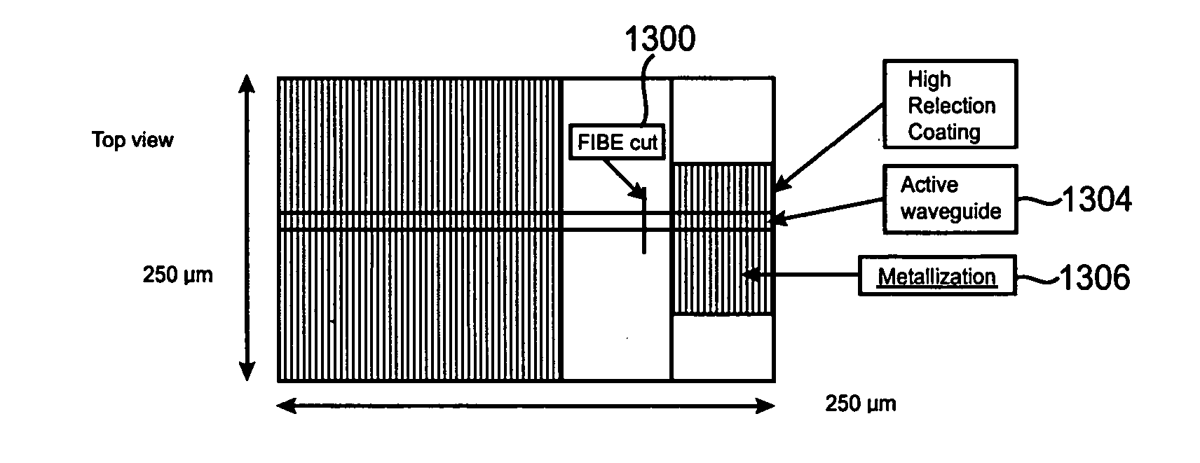
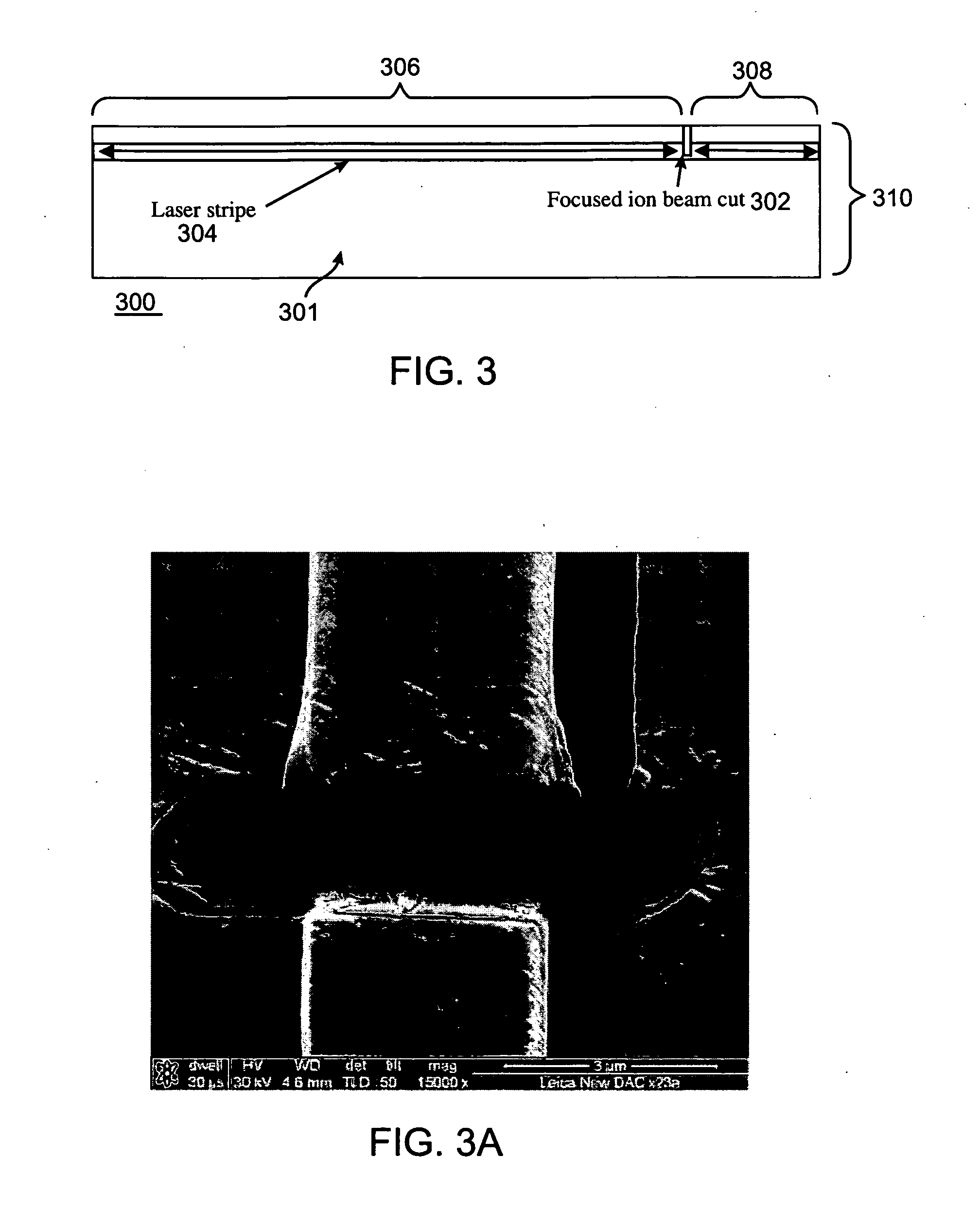
[0055] Embodiments in accordance with the present invention relate to the use of precise etching techniques in the construction of high quality lasers. In accordance with one embodiment of the present invention, Focused Ion Beam Etching (FIBE) of a semiconductor stripe in a multi-mode edge-emitting Fabry-Perot (FP) laser may allow the rapid and effective fabrication of a single mode laser and / or a surface emitting laser. The use of FIBE or other precise etching techniques allows precise control over the dimension, angle, and orientation of etched features, and offers extremely smooth surfaces that reduce optical loss in the resulting device.
[0056] An embodiment of a process in accordance with the present invention utilizes a focused ion beam, such as a focused beam of Gallium ions, to etch pre-designed shapes and cut channels into semiconductor laser stripes in order to produce the desired effects of light emission. Optical devices fabricated in accordance with embodiments of the p...
PUM
 Abstract
Description
Claims
Application Information