

Manufacturing method for semiconductor device
a manufacturing method and semiconductor technology, applied in the direction of coatings, metallic material coating processes, chemical vapor deposition coatings, etc., can solve the problems of inferior film formed by condensation cvd method, and increasing the risk of dielectric film cracking
- Summary
- Abstract
- Description
- Claims
- Application Information
AI Technical Summary
Benefits of technology
Problems solved by technology
Method used
Image

Examples
Embodiment Construction
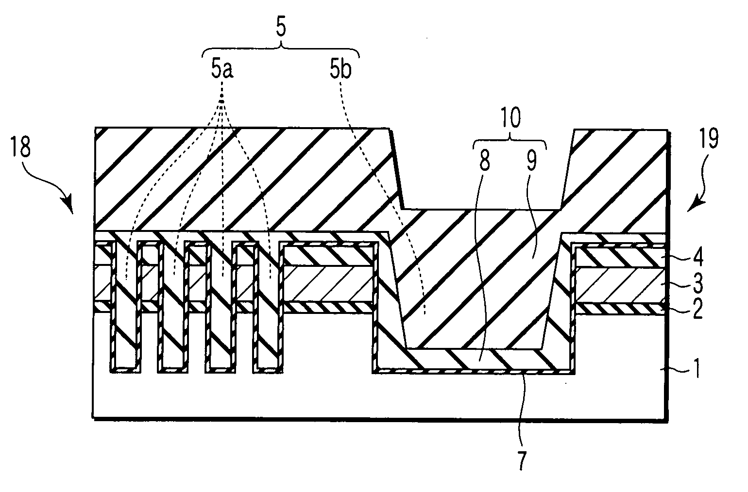
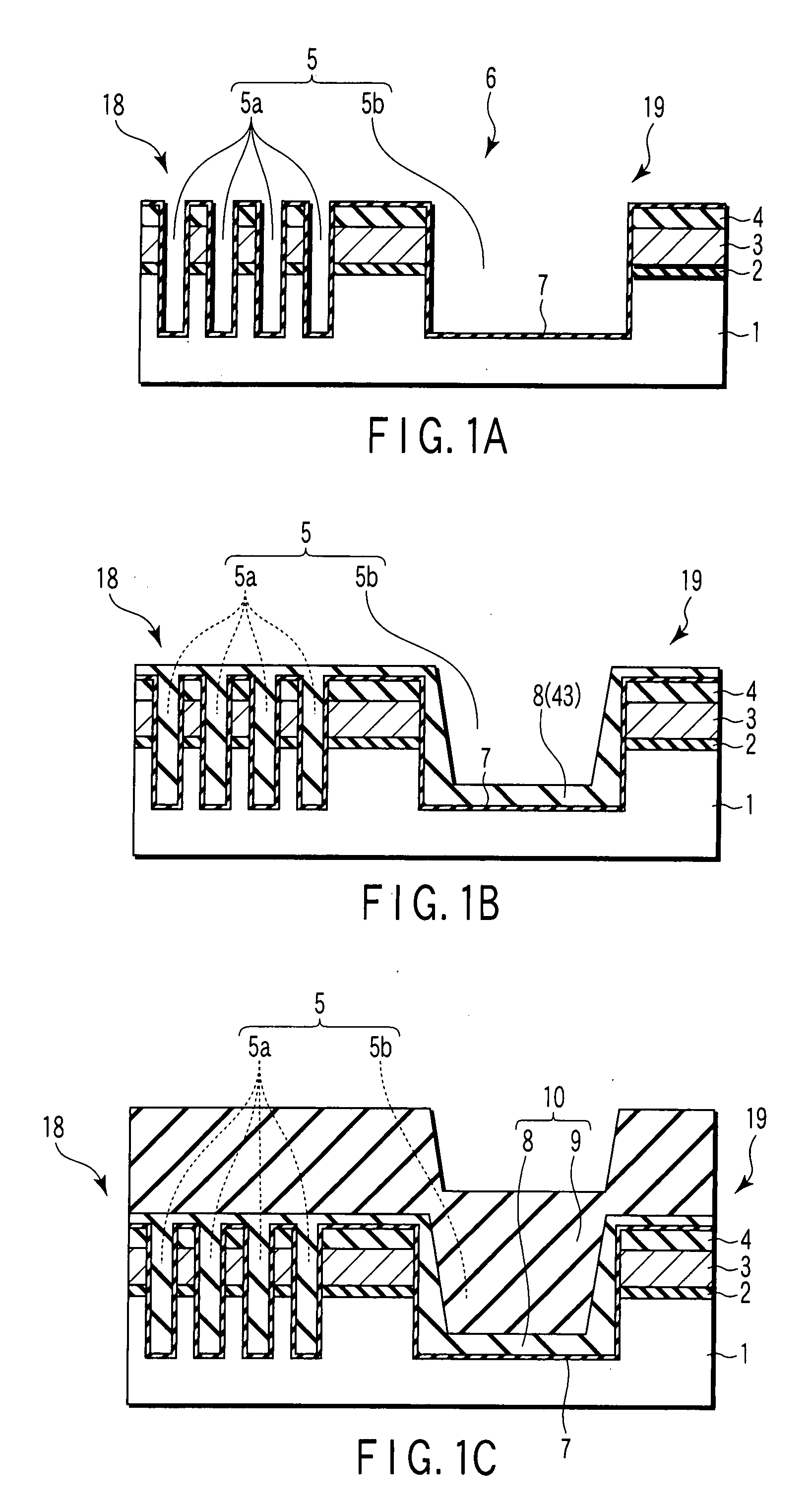
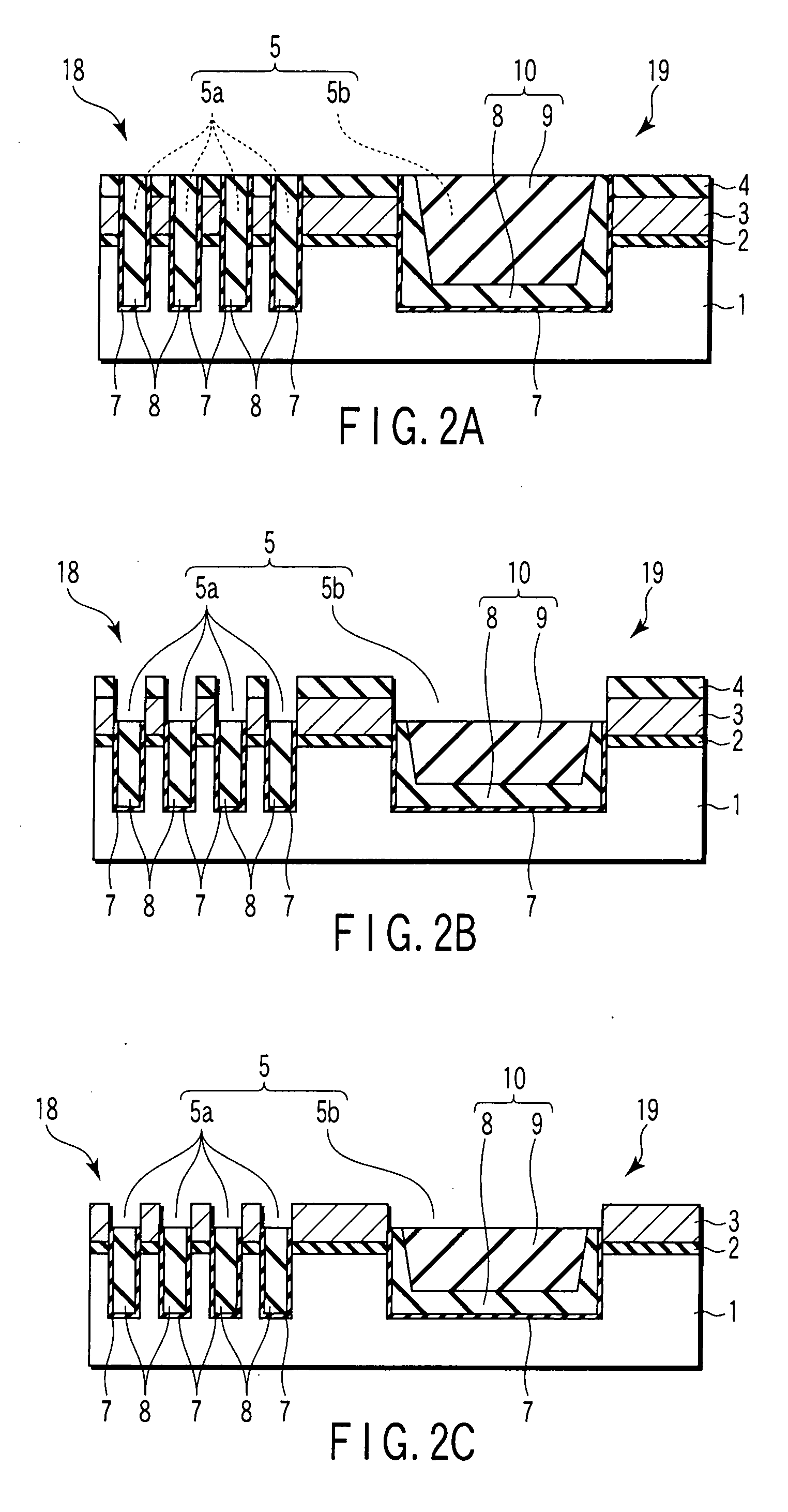
[0012] An embodiment of the invention will be described below with reference to FIGS. 1A to 9D. A technique of burying plural recesses (trenches), made in a superficial portion of a semiconductor substrate and having different aspect ratios, with a dielectric film will be described in the embodiment. Specifically, in the plural recesses made in the superficial portion of the semiconductor substrate included in a flash memory, an inside of the shallow isolation trench (STI) made in a memory cell forming region with a narrow pitch is buried to an upper portion with the dielectric film which is formed by a film forming method called condensation CVD method (described in detail later). On the other hand, the inside of the widely-made trench in a forming region of peripheral circuits except for a memory cell is not fully buried to the upper portion with the dielectric film, but the dielectric film is provided in a lower portion of the inside of the widely-made trench by the condensation ...
PUM
| Property | Measurement | Unit |
|---|---|---|
| Temperature | aaaaa | aaaaa |
| Time | aaaaa | aaaaa |
| Width | aaaaa | aaaaa |
Abstract
Description
Claims
Application Information