Preparation method and preparation device of high-purity metal film and semiconductor chip

A metal film, high-purity technology, applied in semiconductor devices, metal material coating process, coating and other directions, can solve the problems of cumbersome preparation process of high-purity refractory metal film, achieve low cost, low purity requirements, and simple process Effect

Pending Publication Date: 2021-03-16
JIHUA LAB
View PDF2 Cites 2 Cited by
  • Summary
  • Abstract
  • Description
  • Claims
  • Application Information

AI Technical Summary

Problems solved by technology

[0005] In view of the above deficiencies in the prior art, the object of the present invention is to provide a method for preparing a high-purity metal thin film, a preparation device and a semiconductor chip, aiming at solving the problem of the cumbersome preparation process of the existing high-purity refractory metal thin film

Method used


Image

  • Preparation method and preparation device of high-purity metal film and semiconductor chip

Examples


Embodiment 1

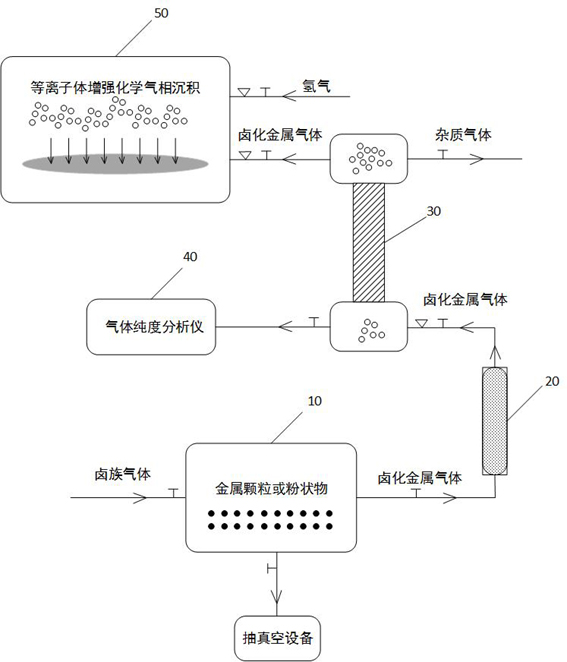
[0073] First, put refractory metal tungsten particles or powder in a vacuum chamber, the diameter of the particles is less than 6mm, vacuumize for 1.6 hours, and the vacuum degree reaches 10 -6 mbar and above;

[0074] Introduce high-purity fluorine gas and tungsten metal for full contact reaction at room temperature, and the reaction time is controlled within 2 hours to obtain tungsten hexafluoride gas;

[0075] The tungsten hexafluoride metal gas obtained after the reaction is conveyed from bottom to top through the adsorption filter device. The filter device is 800mm in height and 60mm in diameter. Activated alumina with a diameter of 3mm is used as the adsorbent for preliminary purification, and the flow rate is controlled at 50sccm ;

[0076] The preliminary purified gas is sent to the rectification tower. The height of the rectification tower is 1500mm and the diameter is 90mm. The temperature at the bottom of the tower is controlled between 17°C and 30°C. The purifica...

Embodiment 2

[0084] First, put refractory metal tantalum particles or powder in a vacuum chamber, the diameter of the particles is less than 5mm, vacuumize for 1 hour, and the vacuum degree reaches 10 -6 mbar and above;

[0085] Introduce high-purity fluorine gas and tantalum metal for full contact reaction at room temperature, and the reaction time is controlled at 1.5 hours to obtain tantalum pentafluoride gas;

[0086] The tantalum pentafluoride gas obtained after the reaction is conveyed from bottom to top through the adsorption filter device. The filter device is 700mm in height and 50mm in diameter, and a mixture of NaF and KF with a diameter of 3mm is used (the mass ratio of NaF and KF is 1: 1) As an adsorbent for preliminary purification, the flow rate is controlled at 50 sccm;

[0087]The preliminary purified gas is sent to the rectification tower. The height of the rectification tower is 800mm and the diameter is 40mm. The temperature at the bottom of the tower is controlled bet...


PUM

PropertyMeasurementUnit
particle diameteraaaaaaaaaa
diameteraaaaaaaaaa
heightaaaaaaaaaa

Abstract

The invention discloses a preparation method and a preparation device of a high-purity metal film and a semiconductor chip. The preparation method comprises the following steps of placing metal particles or powder into a vacuum chamber; feeding high-purity halogen gas into the vacuum chamber to react with the metal particles or powder at normal temperature; carrying out adsorption filtration on halogenated metal gas obtained after the reaction; carrying out rectification and purification by utilizing the boiling point difference between the halogenated metal gas and impurities; and respectively feeding the purified halogenated metal gas and high-purity hydrogen into a plasma enhanced chemical vapor deposition coating equipment chamber, and carrying out deposition to form metal film on a semiconductor substrate. The preparation method of the high-purity metal film is simple in process, low in cost and low in requirement for the purity of raw materials, the raw materials are easy to obtain, and meanwhile the purity of the refractory metal film can be effectively improved.

Description

technical field [0001] The invention relates to the field of metal thin film preparation technology, and mainly relates to a preparation method, a preparation device and a semiconductor chip of a high-purity metal thin film. Background technique [0002] Refractory metals usually refer to metals such as tungsten W, tantalum Ta, molybdenum Mo, niobium Nb, zirconium Zr, titanium Ti and other metals. Such metal materials have high electron migration resistance, high electron emission coefficient, high melting point, and low thermal expansion coefficient. , stable properties, strong corrosion resistance and other advantages, and are widely used in electronics, electricity, strong radiation, high temperature and other fields; especially in the manufacture of semiconductor chips, nano-scale W, Ta, Mo, Nb, Thin films such as Zr and Ti are necessary thin films in semiconductor technology to realize the physical functions of semiconductor chips; they can also be applied to gate circu...

Claims


Application Information

Patent Timeline
Patent Type & Authority Applications(China)
IPC IPC(8): C23C16/448C23C16/505C23C16/511C23C16/08H01L29/45
CPCC23C16/4488C23C16/505C23C16/511C23C16/08H01L29/45
Inventor 郭可升胡琅卫红胡强徐平张翅腾飞姚龙方威
Owner JIHUA LAB
Why Eureka
Try Eureka