Method of forming semiconductor device and semiconductor device

a technology of semiconductor devices and semiconductor films, applied in the direction of semiconductor devices, basic electric elements, electrical apparatus, etc., can solve the problems of increasing the interface layer of high-dielectric-constant insulation films, increasing in-plane variations, and increasing undesirable effects of interface layer deterioration, so as to achieve excellent in-plane uniformity, high film density, and low power consumption

Inactive Publication Date: 2008-12-04
KK TOSHIBA
View PDF15 Cites 2 Cited by
  • Summary
  • Abstract
  • Description
  • Claims
  • Application Information

AI Technical Summary

Benefits of technology

[0020]Therefore, it is an object of the present invention to provide a semiconductor device and a method of forming an ultrathin silicon oxide film having a high film density and excellent in-plane uniformity by suppressing interface roughening occurring during high-temperature oxidation and thermal treatment.
[0027]According to the present invention, in a step of previously forming an interface oxide film of high-dielectric-constant insulation film / silicon oxide film / Si substrate structure, interface roughening during high-temperature oxidation and thermal treatment is suppressed. This makes it possible to form an interface oxide film having a high film density and excellent in-plane uniformity. Thus, a low power-consumption, high-speed, reliable MIS semiconductor device can be offered.

Problems solved by technology

Such an increase is undesirable for the interface layer of the high-dielectric-constant insulation film.
Conversely, if oxidation is performed in an ambient with a low oxygen partial pressure, SiO desorbs from the interface, thus deteriorating the interface and increasing in-plane variations.
Furthermore, low-temperature oxidation leads to a decrease of the film density.
Deterioration of the in-plane uniformity is unavoidable in spite of radical oxidation.

Method used


Image

  • Method of forming semiconductor device and semiconductor device
  • Method of forming semiconductor device and semiconductor device
  • Method of forming semiconductor device and semiconductor device

Examples


Embodiment Construction

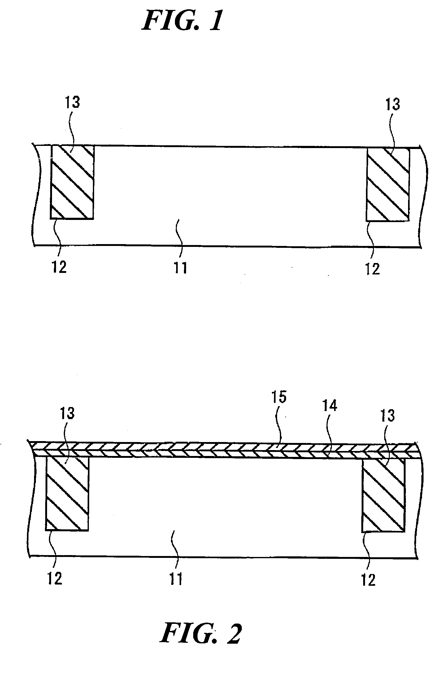
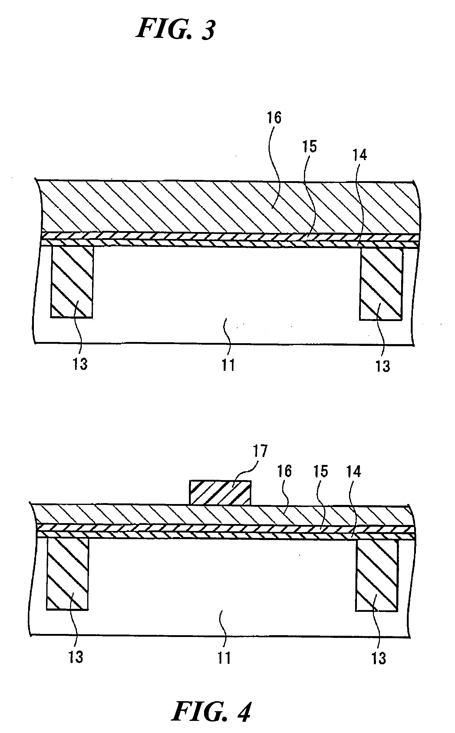
[0039]Referring now to the drawings, wherein like reference numerals designate identical or corresponding parts through out the several views, the present invention will be described.

[0040]Unless specifically defined, all technical and scientific terms used herein have the same meaning as commonly understood by a skilled artisan in microfabrication and semiconductor manufacturing.

[0041]All methods and materials similar or equivalent to those described herein can be used in the practice or testing of the present invention, with suitable methods and materials being described herein. All publications, patent applications, patents, and other references mentioned herein are incorporated by reference in their entirety. In case of conflict, the present specification, including definitions, will control. Further, the materials, methods, and examples are illustrative only and are not intended to be limiting, unless otherwise specified.

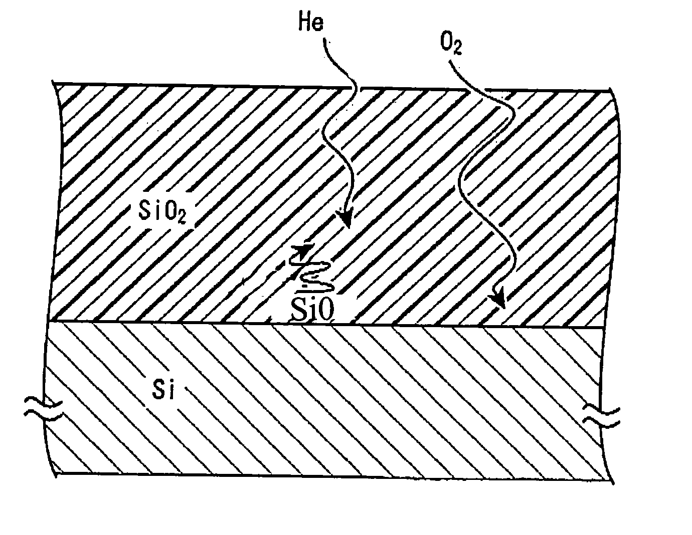
[0042]As a first embodiment of the present invention, a d...


PUM


Abstract

The present invention provides a semiconductor device having an improved silicon oxide film as a gate insulation film of a Metal Insulator Semiconductor structure and a method of making the same.

Description

CROSS-REFERENCE TO RELATED APPLICATIONS[0001]The present application claims priority to Japanese Application No. JP 2002-094150, filed on Mar. 29, 2002, which is hereby incorporated by reference in its entirety.BACKGROUND OF THE INVENTION[0002]1. Field of the Invention[0003]The present invention relates to a semiconductor device having an improved silicon oxide film as a gate insulation film of a Metal Insulator Semiconductor structure and a method of making the same.[0004]2. Discussion of the Background[0005]With the miniaturization of silicon semiconductor integrated circuits the dimensions of MIS (Metal Insulator Semiconductor) semiconductor devices have also decreased. According to ITRS (International Technology Roadmap for Semiconductors; updated version in 2000), the 100-nm technology node needs a gate insulation film having an equivalent oxide thickness (hereinafter abbreviated EOT) of 1.0 to 1.5 nm. At this film thickness, an insulation film having a higher dielectric consta...

Claims


Application Information

Patent Timeline
Patent Type & Authority Applications(United States)
IPC IPC(8): H01L21/31H01L21/316H01L21/28H01L21/314H01L21/318H01L29/51H01L29/78
CPCH01L21/28167H01L21/28185H01L21/28194H01L21/28211H01L21/3144H01L21/31604H01L21/31641H01L21/31645H01L21/31662H01L21/3185H01L29/513H01L29/517H01L29/518H01L21/02189H01L21/02181H01L21/022H01L21/02263H01L21/02238H01L21/0217
Inventor MURAOKA, KOUICHI
Owner KK TOSHIBA
Why Eureka
Try Eureka