Low optical feedback noise self-pulsating semiconductor laser

a semiconductor laser and low optical feedback technology, applied in semiconductor lasers, laser details, electrical equipment, etc., can solve the problems of signal readout error, increased cost, unnecessary radiation (emi: electro-magnetic interference) generation, etc., to achieve stable self-pulsation, improve operation reliability, and reduce operating current

Inactive Publication Date: 2008-01-17
NEC ELECTRONICS CORP
View PDF1 Cites 8 Cited by
  • Summary
  • Abstract
  • Description
  • Claims
  • Application Information

AI Technical Summary

Benefits of technology

[0024]In the self-pulsating semiconductor laser mentioned above, the temperature dependency of the self-pulsation can be adequately taken into account. As a result, the stable self-pulsation can be maintained over a wide temperature range. Since optical feedback noises can be suppressed finely over the entire range of operating temperatures, the operation reliability can be improved. Further, an operating current is reduced, so that the long-term reliability can be improved as well.

Problems solved by technology

The optical feedback noise causes a signal readout error and the like.
Therefore, it is one of the critical issues in the field of semiconductor lasers to suppress the optical feedback noise.
In this case, a high-frequency oscillator is required additionally, thereby increasing the cost.
Further, an unnecessary radiation (EMI: Electro-Magnetic Interference) is generated since the high-frequency current is used.
To mount a component as a measure for dealing with EMI causes more increase in the cost.
Therefore, a self-pulsating operation occurs by the large gain and the loss that is in balance with the gain, so that the volume of the saturable absorber region tends to become large.
However, when the gain determined depending on the structure of the active layer is too small or the lateral spread of the electric current is too narrow, the loss becomes excessive.
Thus, the volume of the saturable absorber region becomes large, thereby weaken the intensity of the self-pulsation.
Therefore, a self-pulsating operation occurs by the small gain and the loss that is in balance with the gain, so that the volume of the saturable absorber region tends to become small.
However, when the gain determined depending on the structure of the active layer is too small so that the loss becomes excessive, or when the lateral spread of the electric current is too large so that the gain becomes excessive, the volume of the saturable absorber region becomes small.
However, such temperature dependency of the self-pulsation is not sufficiently considered in the above mentioned related techniques.
This induces signal reproduction errors caused by optical feedback noises, which is not preferable in terms of the reliability of the products.
Especially, it is required for a semiconductor laser used in an optical disk device to perform stable self-pulsation over a wide temperature range of about −10° C. to 75° C. It is difficult with the above mentioned related techniques to achieve the stable self-pulsation over such wide range of temperatures.

Method used


Image

  • Low optical feedback noise self-pulsating semiconductor laser
  • Low optical feedback noise self-pulsating semiconductor laser
  • Low optical feedback noise self-pulsating semiconductor laser

Examples


first embodiment

1. First Embodiment

1-1. Structure

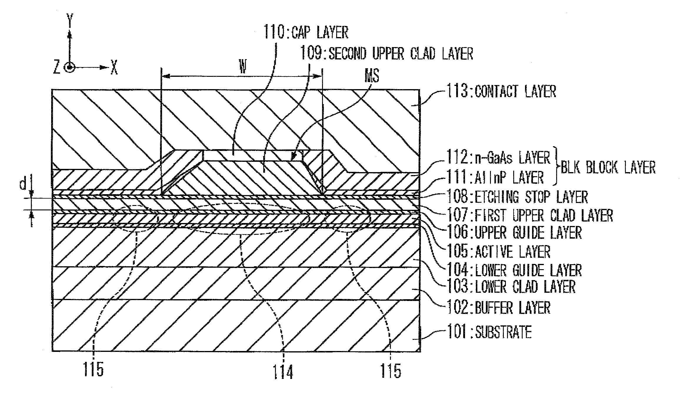
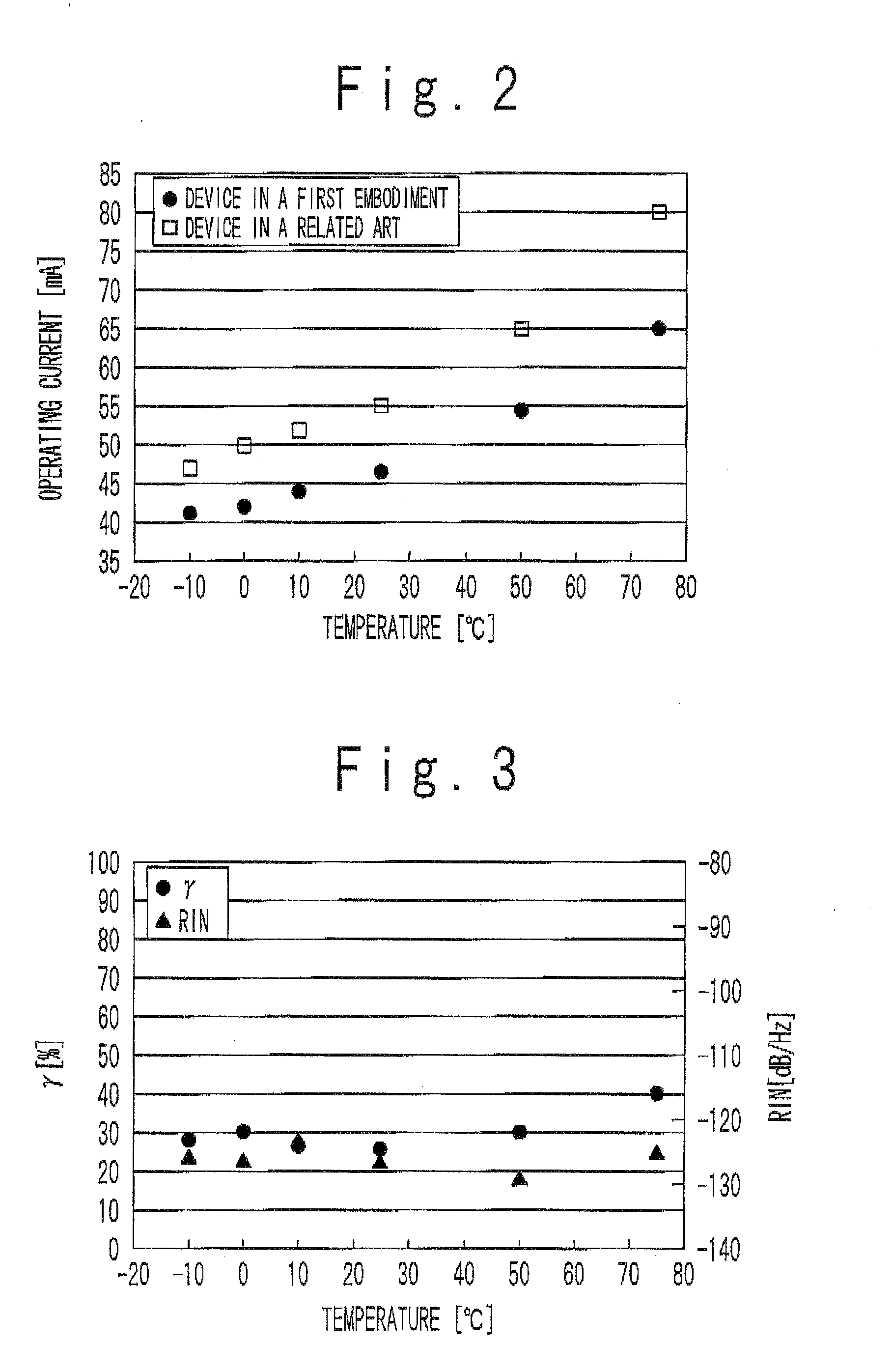
[0050]FIG. 1 is a sectional view showing a structure of a self-pulsating semiconductor laser according to a first embodiment of the present invention. In FIG. 1, the Z-direction is an axial direction of a cavity, and the X-direction (horizontal direction) is a direction that is orthogonal to the axial direction of the cavity and in parallel to a p-n junction face. The Y-direction is a direction that is orthogonal to the axial direction of the cavity and vertical to the pn-junction face. The standing waves that appear in the X, Y, and Z directions are called a horizontal transverse mode, a vertical transverse mode, and a longitudinal mode, respectively.

[0051]In FIG. 1, a first conductivity type buffer layer 102 for improving a crystalline property is formed on a first conductivity type semiconductor substrate 101. A “double heterostructure (DH)” is formed on the buffer layer 102. Specifically, an active layer 105 is formed on a first conductivity type...

second embodiment

2. Second Embodiment

[0099]FIG. 9 is a sectional view showing the structure of a self-pulsating semiconductor laser according to a second embodiment of the present invention. In FIG. 9, the same reference numerals are applied to the structure elements that are same as those of FIG. 1, and redundant explanations are omitted as appropriate.

[0100]The block layer BLK according to the present embodiment is constituted only with a first-conductive (AlxGa1-x)0.5In0.5P layer 120 without an GaAs layer. For example, the block layer BLK includes an n-type AlInP layer 120 (x=1). The thickness of the n-type AlInP layer 120 is 1000 nm, for example, and the impurity density is 3×1018 cm−3, for example. With such structure, it is possible to obtain the same effects as those of the first embodiment. The manufacturing method of the semiconductor laser element according to the present embodiment is the same as that of the first embodiment.

third embodiment

3. Third Embodiment

[0101]In the case presented in the first embodiment, the semiconductor laminated structure on the semiconductor substrate 101 is formed with a GaInP / AlGaInP type material, and the emission wavelength is about 650 nm. The present invention is also effective for a self-pulsating semiconductor laser in which the semiconductor laminated structure is formed with a GaAs / AlGaAs type material, and the emission wavelength is about 780 nm. FIG. 10 shows the structure of such self-pulsating semiconductor laser. Explanations that overlap with those of the above-described embodiments are omitted as appropriate. Examples of each layer shown in FIG. 10 will be explained below.

[0102]Semiconductor substrate 301: n-type GaAs

[0103]Buffer layer 302: n-type GaAs; thickness=650 nm; impurity concentration=5×1017 cm−3

[0104]Lower clad layer 303: n-type AlGaAs (x=0.5); thickness=1200 nm impurity concentration=1×1018 cm−3

[0105]Lower guide layer 304: AlGaAs (x=0.34); thickness=80 nm

[0106]M...


PUM


Abstract

A self-pulsating semiconductor laser includes a lower clad layer formed on a semiconductor substrate, an active layer formed on the lower clad layer, the first upper clad layer formed on the active layer, a second upper clad layer formed on the first upper clad layer and a block layers. The second upper clad layer has a mesa structure. The block layers are formed on both sides of the second upper clad layer and includes a layer the bandgap thereof is larger than that of the active layer. When a self-pulsation is performed, saturable absorber regions are formed on the both sides of a gain region. The thickness d of the first upper clad layer satisfies a relation 220 nm≦d≦450 nm. A stable self-pulsation can be achieved in a wide temperature range.

Description

BACKGROUND OF THE INVENTION[0001]1. Field of the Invention[0002]The present invention relates to a semiconductor laser and a manufacturing method thereof. More specifically, the present invention relates to a self-pulsating semiconductor laser that is excellent in suppressing an optical feedback noise, and to a manufacturing method thereof.[0003]2. Description of Related Art[0004]The semiconductor laser is used for light sources in optical disk devices, optical fiber communications, optical arithmetic operations and the like. In a case of an optical disk device such as a DVD device, there is possibility that reflected light from an optical disk makes incident again back on the semiconductor laser element. The light making incident back again on the element is called as feedback light, and a noise generated in the output of the emission light because of the feedback light is called an optical feedback noise. The optical feedback noise causes a signal readout error and the like. There...

Claims


Application Information

Patent Timeline
Patent Type & Authority Applications(United States)
IPC IPC(8): H01S5/343H01S5/00
CPCB82Y20/00H01S2301/18H01S5/2206H01S5/222H01S5/2222H01S5/2224H01S5/2231H01S5/305H01S5/3054H01S5/3211H01S5/3432H01S5/34326H01S5/3436H01S5/4087H01S2301/02H01S5/065H01S5/00
Inventor KOBAYASHI, MASAHIDE
Owner NEC ELECTRONICS CORP
Why Eureka
Try Eureka