

Surface inspection method and surface inspection apparatus
a surface inspection and surface technology, applied in the direction of mechanical measurement arrangements, mechanical roughness/irregularity measurements, instruments, etc., can solve the problems of typical worse time response characteristic of the photomultiplier tube, existing crystal defects, rough surface of the substrate, etc., to eliminate or reduce its influence
- Summary
- Abstract
- Description
- Claims
- Application Information
AI Technical Summary
Benefits of technology
Problems solved by technology
Method used
Image

Examples
Embodiment Construction
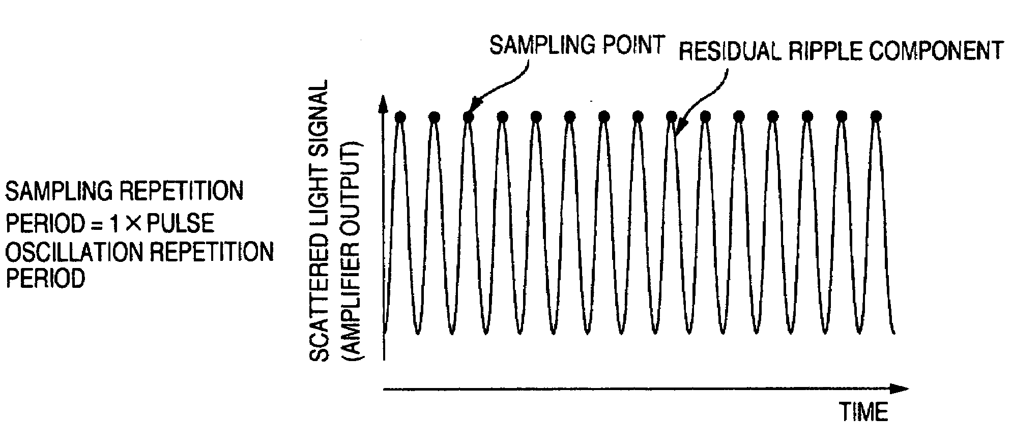
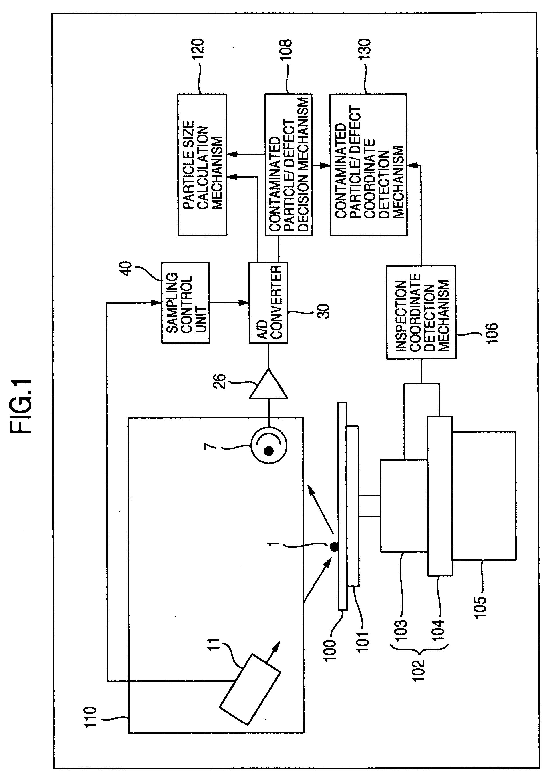
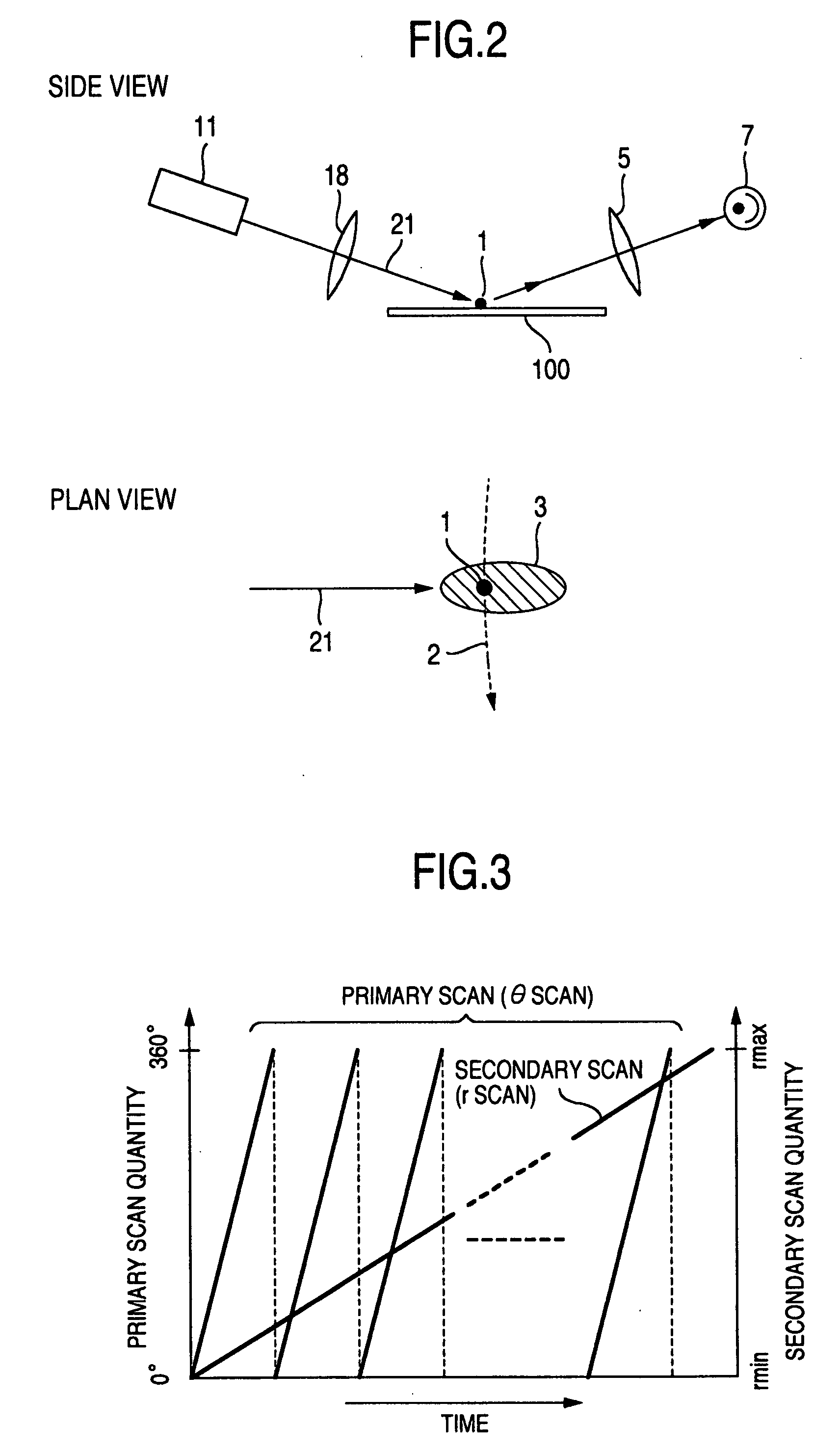
[0038]The present invention relates to a technique for detecting a minute contaminated particle or defect when it is present on, for example, a semiconductor substrate (semiconductor wafer), and a technique for measuring information concerning surface roughness of the substrate. In particular, the present invention relates to a surface inspection technique for inspecting the substrate surface by using a pulse laser, which performs pulse oscillation repetitively in time, as the light source.
[0039]A surface inspection apparatus according to an embodiment of the present invention includes an object to be inspected moving stage, a pulse laser light source, illumination means for irradiating an illumination region having a predetermined size on the surface of an object to be inspected with laser light emitted from the pulse laser light source, scattered / diffracted / reflected light collecting means for collecting light generated by scattering / diffracting / reflecting the irradiated light in ...
PUM
| Property | Measurement | Unit |
|---|---|---|
| wavelength | aaaaa | aaaaa |
| oscillation wavelength | aaaaa | aaaaa |
| frequency | aaaaa | aaaaa |
Abstract
Description
Claims
Application Information