
Structure and method for improving shielded gate field effect transistors

a gate field effect transistor and shielded gate technology, applied in the direction of transistors, semiconductor devices, electrical equipment, etc., can solve the problems of increasing gate-to-drain capacitance, increasing power dissipation, and reducing on-resistance, so as to reduce reverse recovery loss

Active Publication Date: 2008-01-24
SEMICON COMPONENTS IND LLC
View PDF25 Cites 71 Cited by
  • Summary
  • Abstract
  • Description
  • Claims
  • Application Information

AI Technical Summary

Benefits of technology

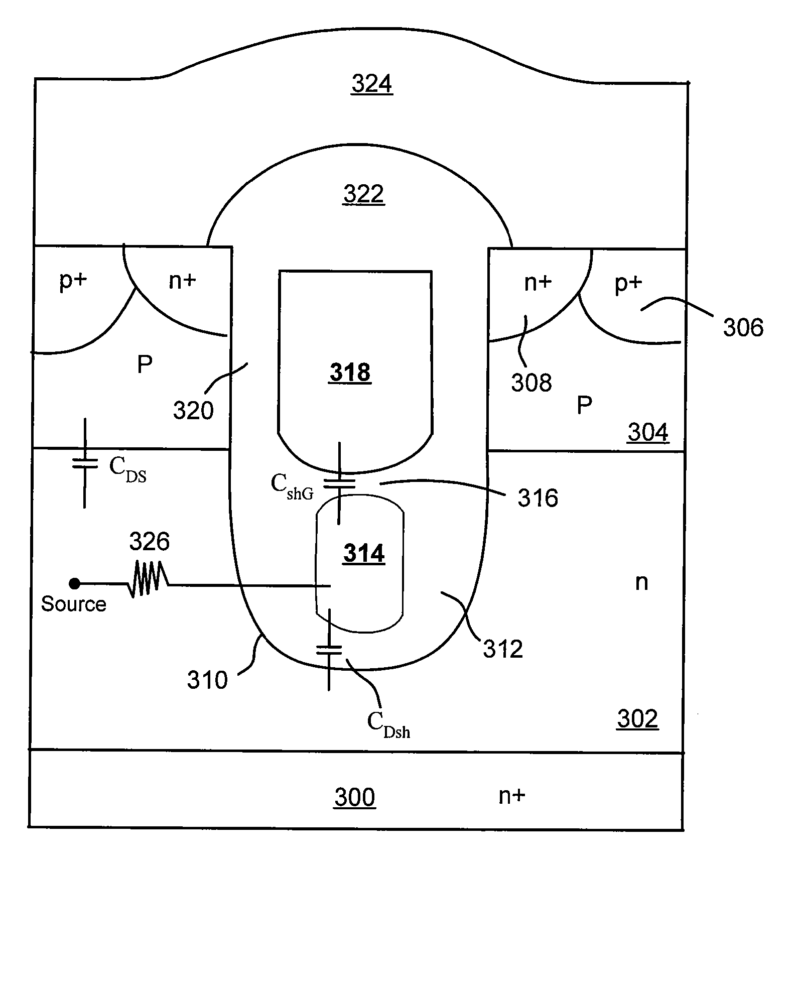
[0005] Various embodiments of the present invention provide shielded gate trench transistors with reduced reverse recovery loss. In accordance with one embodiment of the invention, a field effect transistor includes a trench extending into a drift region of the field effect transistor. A shield electrode in a lower portion of the trench is insulated from the drift region by a shield dielectric. A gate electrode is formed in the trench atop the shield electrode and insulated therefrom by an inter-electrode dielectric. A resistive element is coupled between the shield electrode and a source region of the transistor. The inclusion of the resistive element reduces the reverse recovery charge by enabling the voltage on the shield electrode to increase in response to a relatively small charge that develops on the shield capacitor due to the increasing potential in the drain.

Problems solved by technology

In particular, the placement of many trenches in a channel decreases the on-resistance but also increases the gate-to-drain capacitance.
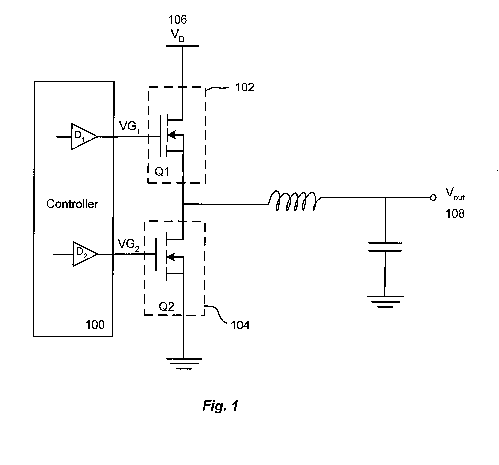
However, for the low-side switch which operates as a synchronous rectifier, excessive charge during the reverse recovery of the body diode results in increased power dissipation and reduced converter efficiency.

Method used


Image

  • Structure and method for improving shielded gate field effect transistors
  • Structure and method for improving shielded gate field effect transistors
  • Structure and method for improving shielded gate field effect transistors

Examples


Embodiment Construction

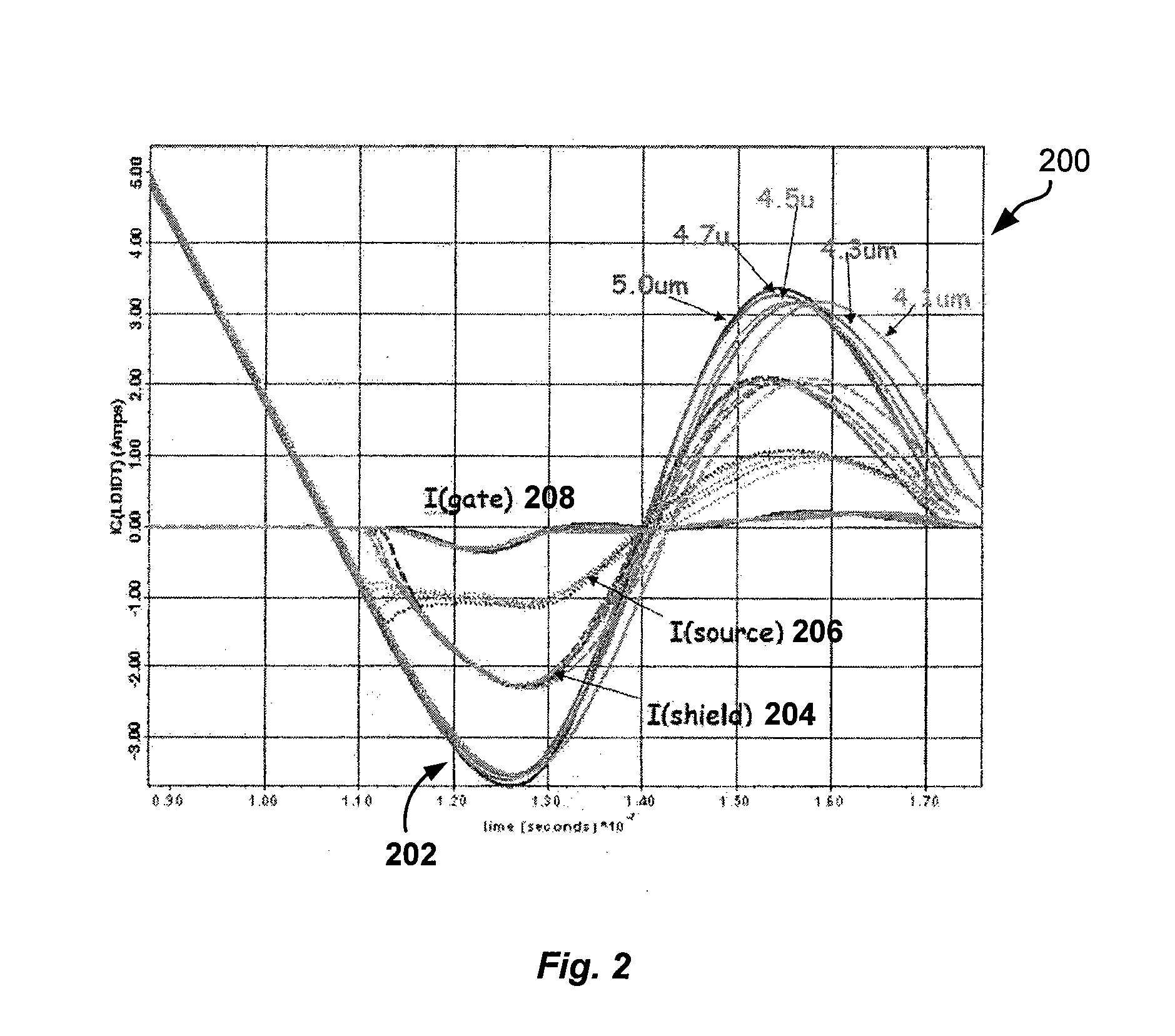
[0022] Diode reverse recovery refers to the process whereby the minority carrier charge stored in the drift region is removed so that the p-n junction diode can be switched from forward to reverse bias. In the context of a shielded gate trench MOSFET, the inventors have found that the displacement current in the shield electrode contributes significantly to the reverse recovery of the body diode. This displacement current is due to the capacitor formed between the drift or drain region and the shield electrode, referred to herein as CDsh. The magnitude of the charge associated with the shield displacement current can be comparable to that of the charge expected from the diode's recovery current alone. Thus, the use of an integrated Schottky diode as described in commonly-owned U.S. Pat. No. 6,351,018 would provide little if any improvement in the diode recovery since any reduction in the total reverse recovery charge would be offset by the shield electrode's contribution to this cha...


PUM


Abstract

A field effect transistor is disclosed. In one embodiment, the field effect transistor includes a trench extending into a drift region of the field effect transistor. A shield electrode in a lower portion of the trench is insulated from the drift region by a shield dielectric. A gate electrode in the trench over the shield electrode is insulated from the shield electrode by an inter-electrode dielectric. A source region is formed adjacent the trench. A resistive element is coupled to the shield electrode and to a source region in the field effective transistor.

Description

CROSS-REFERENCES TO RELATED APPLICATIONS [0001] This application claims the benefit of U.S. Provisional Application No. 60 / 756,835, filed Jan. 5, 2006, which disclosure is incorporated herein by reference in its entirety for all purposes.BACKGROUND OF THE INVENTION [0002] The present invention relates in general to semiconductor power field effect transistors (FETs) and in particular to shielded gate trench MOSFETs with improved reverse recovery currents. [0003] Shielded gate trench MOSFETs provide unique advantages over conventional MOSFETs, such as reduced gate-to-drain capacitance Cgd, reduced on-resistance RDSon, and increased breakdown voltage of the transistor. In particular, the placement of many trenches in a channel decreases the on-resistance but also increases the gate-to-drain capacitance. The shielded gate structure solves this problem by shielding the electric field in the drift region from the gate, thereby substantially reducing the gate-to-drain overlap capacitance....

Claims


Application Information

Patent Timeline
IPC IPC(8): H01L29/78H01L21/336
CPCH01L29/407H01L29/7813H01L29/7803
Inventor SAPP, STEVENCHALLA, ASHOKKOCON, CHRISTOPHER B.
Owner SEMICON COMPONENTS IND LLC
Learn More