A high-robust fast-recovery super-junction power semiconductor transistor and its preparation method
A power semiconductor, highly robust technology, applied in semiconductor/solid-state device manufacturing, semiconductor devices, electrical components, etc., can solve the performance damage of superjunction trench MOSFET devices, increase hole injection efficiency, and increase reverse recovery loss and other problems to achieve the effect of reducing the number of storage carriers, improving reverse recovery characteristics, and reducing reverse recovery losses
- Summary
- Abstract
- Description
- Claims
- Application Information
AI Technical Summary
Problems solved by technology
Method used
Image
Examples
Embodiment 1
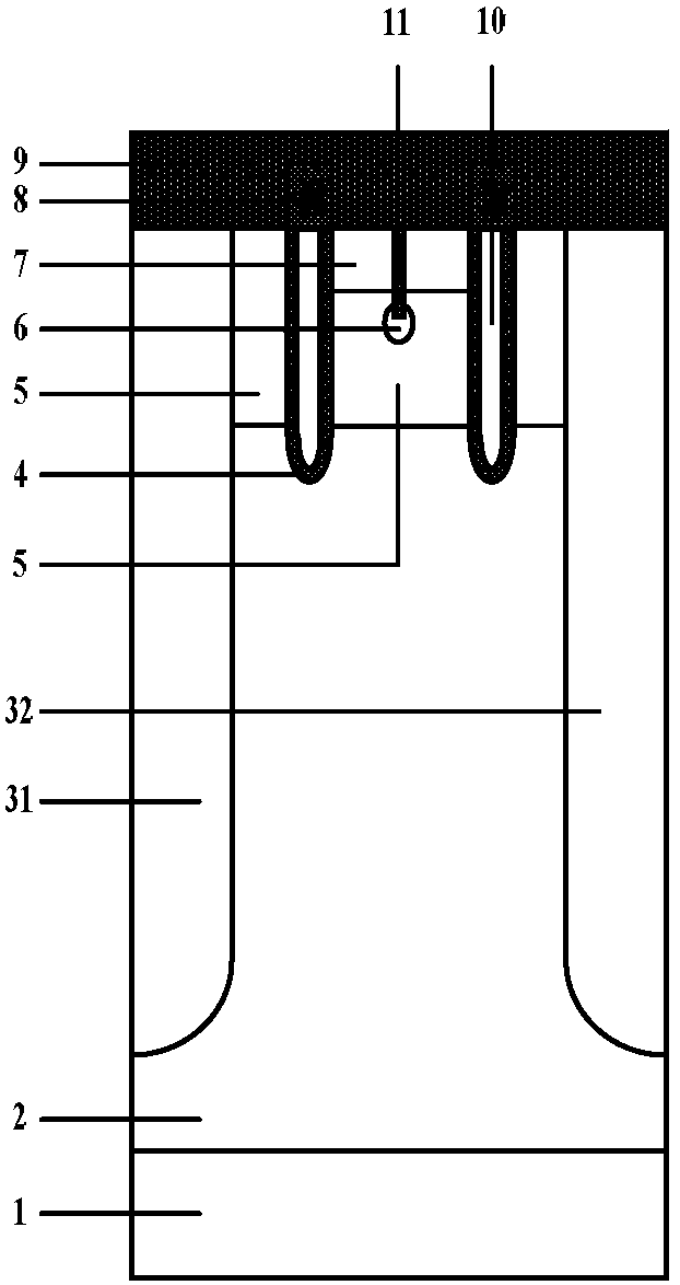
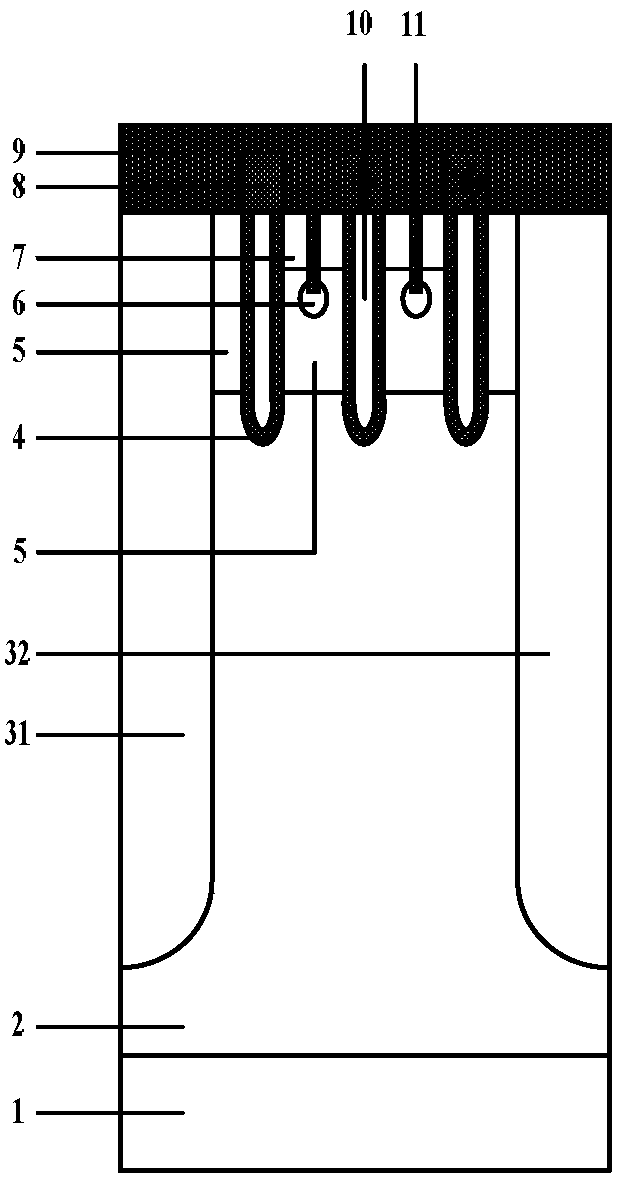
[0034] Combine below Figure 1-2 , to describe the present invention in detail, a high-robust fast recovery super junction power semiconductor transistor, comprising: N-type drain 1, N-type epitaxial layer 2 is arranged on N-type drain 1, N-type epitaxial layer 2 A first strip-shaped P-type body region 31 and a second strip-shaped P-type body region 32 are respectively arranged inside, a first P-type body region 5 is arranged above the N-type epitaxial layer 2, and the first P-type body region 5 Extending from the first strip-shaped P-type body region 31 to the second strip-shaped P-type body region 32, at least two trench gates, heavily doped N-type source electrodes 7 and the first P-type body region 5 are provided. Two P-type body regions 6, the trench gate vertically runs through the first P-type body region 5 and the lower end of the trench gate extends into the N-type epitaxial layer 2, and a first field is provided at the upper end of the trench gate Oxide layer 8, the...
Embodiment 2
[0036] A method for preparing a high-robust fast-recovery superjunction power semiconductor transistor, characterized in that:
[0037] The first step: first select N-type silicon material as the substrate and epitaxially grow N-type epitaxial layer 2;
[0038] Step 2: Next, fabricate high-robust fast-recovery super-junction power semiconductor transistors. First, use a mask to etch deep trenches on the N-type epitaxial layer 2;
[0039] Step 3: Next, fill the deep trench with silicon containing P-type impurities and diffuse the impurity ions to form the first strip-shaped P-type body region 31 and the second strip-shaped P-type body region 31 in the N-type epitaxial layer 2. Strip-shaped P-type body region 32;
[0040] Step 4: Next, between the first strip-shaped P-type body region 31 and the second strip-shaped P-type body region 32, a mask is used to etch a plurality of gate trenches on the N-type epitaxial layer 2;
[0041] Step 5: Next, a gate oxide layer 4 is grown on ...
PUM
 Abstract
Description
Claims
Application Information


