

Liquid display device and fabrication method thereof
- Summary
- Abstract
- Description
- Claims
- Application Information
AI Technical Summary
Benefits of technology
Problems solved by technology
Method used
Image

Examples
example 1
[0078]Example 1 is a specific example for the constituent material used in a liquid crystal display according to the invention and characteristics thereof, as well as for the contents of the processing.
[Material]:
[0079]Fine TiO2 particle slurry manufactured by Tayca Corp. was added to a commercially available heat resistant transparent photosensitive protective film (Optomer PC452 manufactured by JSR). According to the material safety data sheet (MSDS), Optomer PC452 manufactured by JSR comprises an acrylic resin as a base polymer, naphthoquinone diazido sulfonic acid ester as a photosensitizer, and diethylene glycol methylethyl ether as a solvent and has a solid concentration of 32%. The TiO2 slurry manufactured by Tayca Corp. comprises rutile type fine TiO2 particles (grain size: 20 nm) of less photocatalyst activity dispersed in propylene glycol monomethylethyl ether(PGMEA) as the solvent. The periphery of TiO2 is covered with stable SiO2 and further coated at the periphery there...
example 2
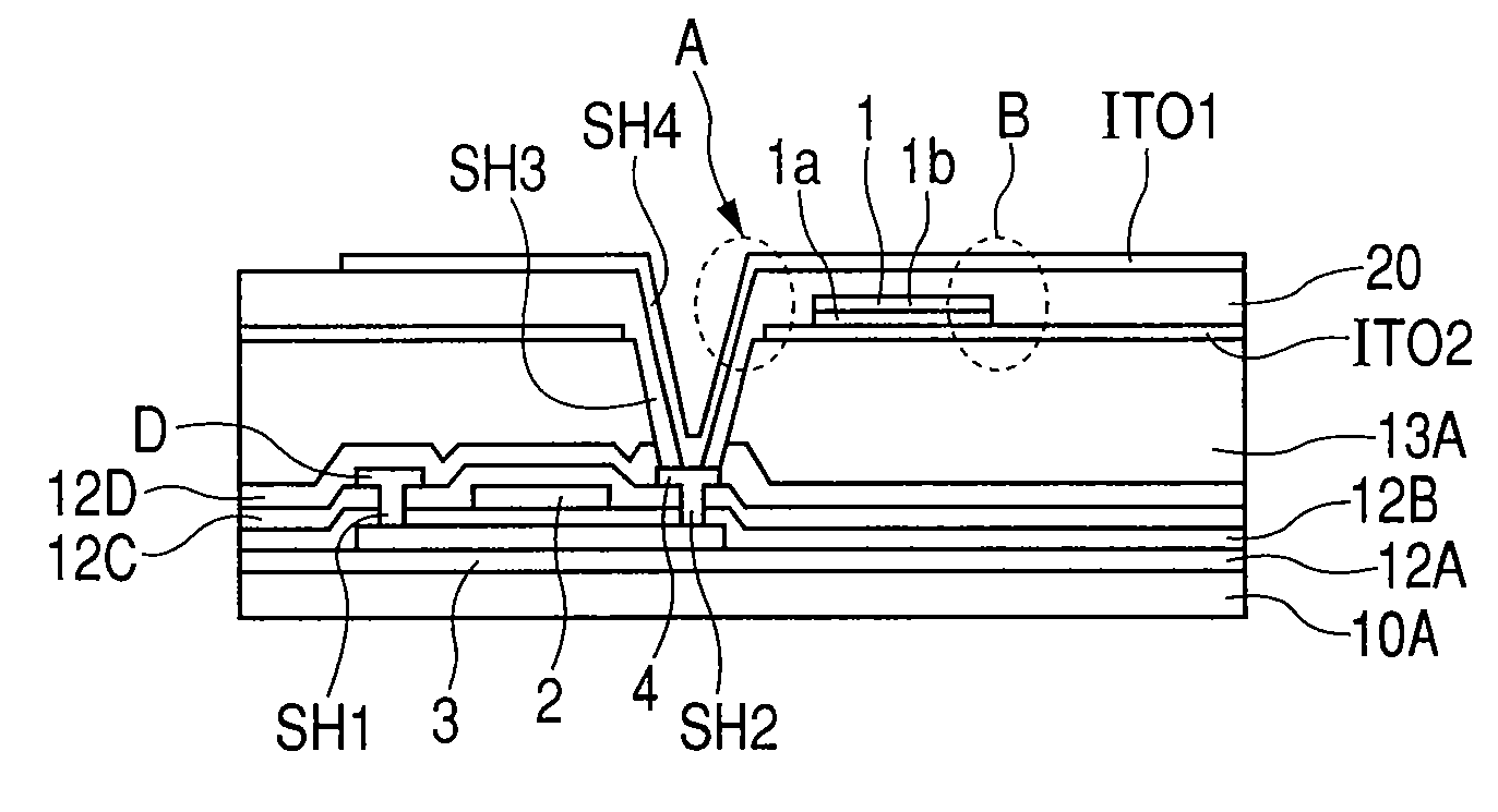
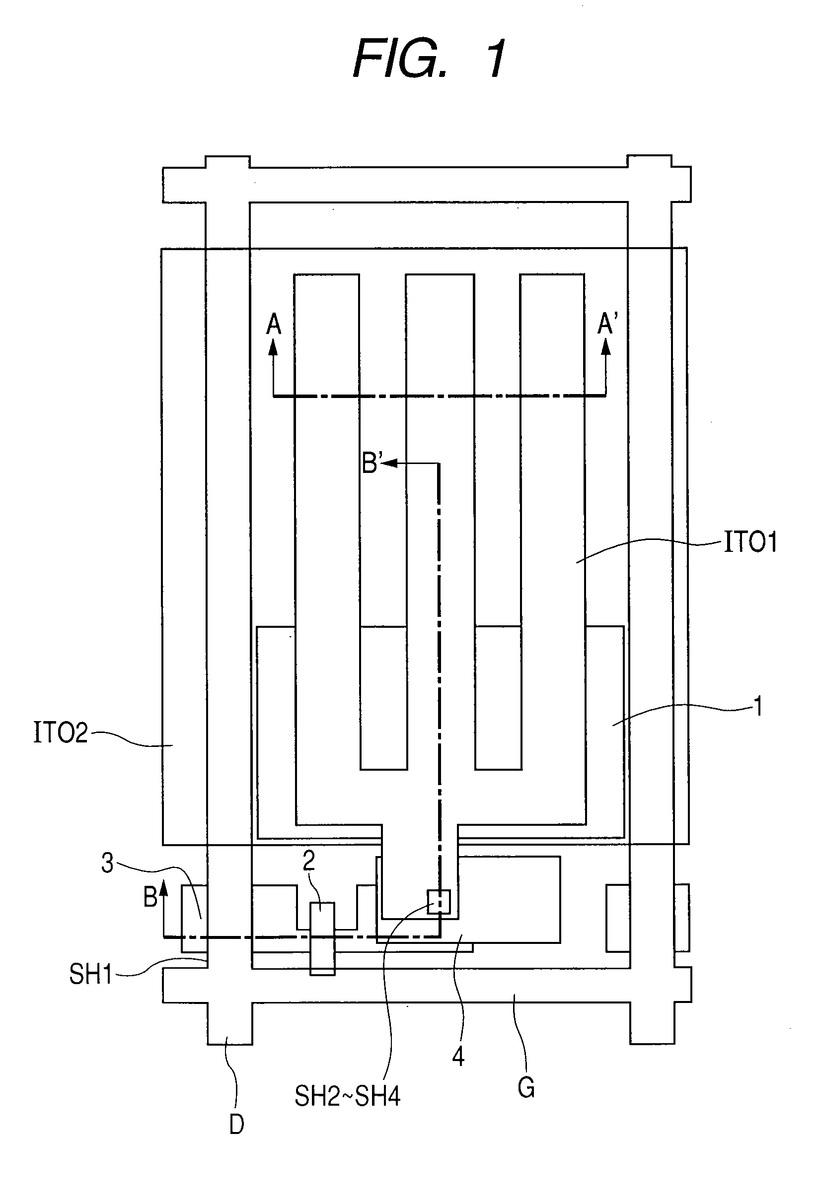
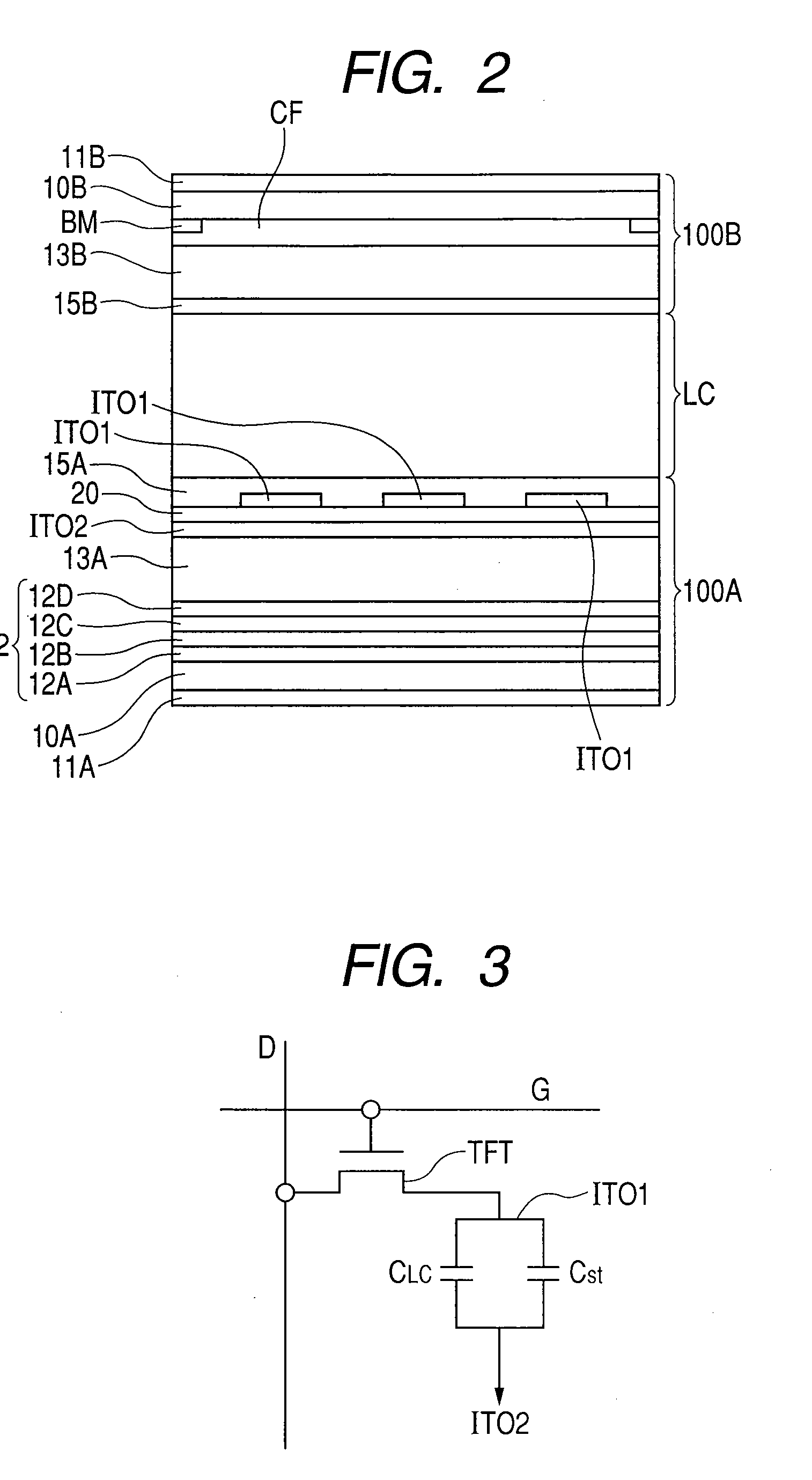
[0087]FIG. 1 is a plan view showing the constitution of a 1 sub-pixel of a liquid crystal display panel according to Example 2 of the invention. FIG. 2 is a cross sectional view showing a cross sectional structure along line A-A′ in FIG. 1. The liquid crystal display panel of Example 2 is an IPS system liquid crystal display panel using a planar counter electrode. As shown in FIG. 2, it has a transparent substrate (100B) and a transparent substrate (100A) opposed to each other by way of a liquid crystal layer LC. In Example 2, the surface side of the transparent substrate (100B) is a view side.
[0088]The transparent substrate (100B) has a glass substrate 10B. On the side of the liquid crystal layer LC of the glass substrate 10B, a light shielding layer (BM), color filter layer (CF), an over coating layer 13B, and an aligned film 15B are formed successively from the glass substrate 10B to the liquid crystal layer LC. Further, a polarizer 11B is formed to the outside of the transparent...
example 3
[0119]In each of the following examples, description is to be made for specific examples of the materials for the transparent film for forming the capacitance. In Example 3, like in Example 1, fine particles or sol-gel of a high dielectric constant material shown in Table 3 were added to a commercially available heat resistant transparent photosensitive protective film (for example, Optomer PC452 manufactured by JSR) at the mixing ratio in Table 3 to form coatable transparent insulating film having a specific dielectric constant of 4.0 or higher. In this case, the mixing ratio (x / y) for Optomer (x) / fine particle or sol-gel (y) is shown by the solid concentration. Samples No. 2-1 to No. 2-12 in Table 3 were evaluated for the characteristics in the same manner as in Example 1 and the results are shown in Table 4.
[0120]As shown in Table 4, lowering of the sensitivity was sometimes observed compared with a case of adding nothing. Particularly, lowering of the sensitivity was observed in...
PUM
 Abstract
Description
Claims
Application Information