Method for manufacturing lower substrate of liquid crystal display device

a liquid crystal display device and manufacturing method technology, applied in the direction of semiconductor devices, basic electric elements, electrical equipment, etc., can solve the problems of reducing the mask step, reducing the manufacturing cost, and the tapered angle is too large, so as to improve the tapered angle of the insulating layer, improve the electric property, and improve the semiconductor layer tapered angle

Inactive Publication Date: 2008-01-24
AU OPTRONICS CORP
View PDF4 Cites 7 Cited by
  • Summary
  • Abstract
  • Description
  • Claims
  • Application Information

AI Technical Summary

Benefits of technology

[0014]The object of the present invention is to provide a manufacturing method of a lower substrate of a TFT-LCD device, which can improve the tapered angles of the semiconductor layer and the insulating layer of a thin film transistor. In addition to forming an improved tapered angle of the insulating layer via dry etching, the barrier layer, the semiconductor layer, the insulating layer and the other layers in a multilayered structure can also be patterned via dry etching. The barrier layer can improve the electric property and the adhesion between layers and the insulating layer with an improved tapered angle can inhibit the formation of manufacturing defects in the following process. Furthermore, in the method of the present invention, the insulating layer in the light-penetrating region of the lower substrate of an LCD device can be etched thoroughly to enhance the light transmittance of the lower substrate and the improved tapered angles of the semiconductor layer and the insulating layer are formed.

Problems solved by technology

Since the manufacturing process is time-consuming and complicated, many defects occur and the manufacturing cost increases.
Hence, issues for reducing the mask steps and simplifying the process are very importance for manufacturing a TFT array substrate.
However, the tapered angle is too large owing to the significant drop of the film-height in the multilayered structure.
However, the tapered angles of most films formed by conventional etching are over the acceptable range.
However, the improved wet etching or dry etching still cannot meet the requirements of excellent tapered angles, reducing manufacturing cost, simplifying process, and / or mass production for manufacturing.

Method used


Image

  • Method for manufacturing lower substrate of liquid crystal display device
  • Method for manufacturing lower substrate of liquid crystal display device
  • Method for manufacturing lower substrate of liquid crystal display device

Examples


embodiment 1

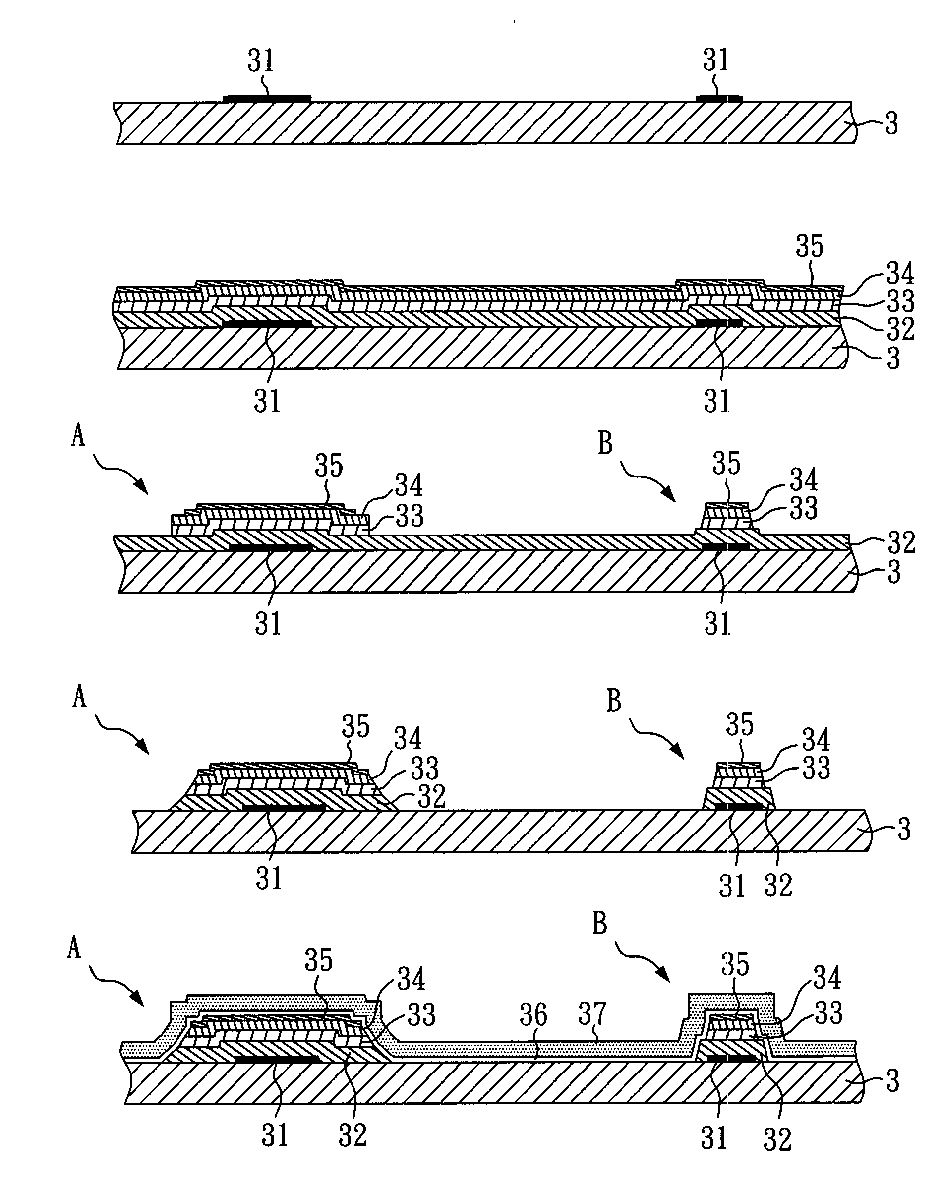
[0041]With reference to FIGS. 3(a) to 3(h), there are shown schematic views of fabricating a lower substrate of a liquid crystal display device of the present embodiment of the present invention. In the embodiment of the present invention, the lower substrate of a TFT-LCD device is prepared by four mask steps.

[0042]As shown in FIG. 3(a), a glass substrate 3 is prepared, and a first metal layer 31 is formed on the glass substrate 3. A pattern of the gate is defined by the first mask process and etching process. Preferably, the first metal layer 31 is composed of chromium alloy and molybdenum, and the structure can be a monolayer structure or a multilayered structure (not shown).

[0043]Then, as shown in FIG. 3(b), an insulating layer 32, a semiconductor layer 33, an ohmic contact layer 34, and a barrier layer 35 are deposited over the patterned first metal layer 31; wherein the insulating layer 32 is silicon oxide, the semiconductor layer 33 is amorphous silicon, the ohmic contact laye...

embodiment 2

[0055]In the present embodiment, the manufacturing process of a lower substrate of a TFT-LCD device is the same as that of Embodiment 1 using a four-stage mask process, except that the semiconductor layer is a multilayer structure and the etching condition of the insulating layer is modified.

[0056]The semiconductor layer of the present embodiment is a multilayered structure comprising a low-deposition-rate Si layer and a high-deposition-rate Si layer. The multilayer structure of the lower substrate is established by depositing a first metal layer, a first insulating layer, a low-deposition-rate Si layer, a high-deposition-rate Si layer, an ohmic contact layer, and a barrier layer in sequence over the substrate.

[0057]In the present embodiment, forming a high-deposition-rate Si layer can reduce the time of depositing a semiconductor layer and increase the efficiency of manufacturing a lower substrate. In addition, the high-deposition-rate Si layer can thicken the semiconductor layer a...

embodiment 3

[0065]In the present embodiment, the manufacturing process of a lower substrate of a TFT-LCD device is the same as that of Embodiment 2 with a four-stage mask process, except that the semiconductor layer is a monolayer structure illustrated in Embodiment 1, and the others, such as the etching gas and the other layer structures of the transistor are similar to those in Embodiment 2.


PUM


Abstract

A method for improving the tapered angles of the insulating layer and the semiconductor layer of a lower substrate of a thin film transistor liquid crystal display device is disclosed. The method mainly applies an etching gas including a sulfur fluoride compound to etch the insulating layer. After etching, the tapered angle of the insulating layer is improved. Moreover, since the etching gas including a sulfur fluoride compound also results in lateral etching on the semiconductor layer, the step coverage of the subsequent process is improved, too. The method of the present invention can also be applied for manufacturing a multilayered thin film transistor containing a barrier layer, a semiconductor layer, and an insulating layer without delamination, breakage, or collapse. In addition, since the number of the used masks is reduced in the method of the present invention, the cost can be reduced and the process can be simplified.

Description

BACKGROUND OF THE INVENTION[0001]1. Field of the Invention[0002]The present invention relates to a method for manufacturing a thin film transistor (TFT), and more particularly, to a method for manufacturing a lower substrate of a liquid crystal display device.[0003]2. Description of Related Art[0004]A thin film transistor liquid crystal display (TFT-LCD) mainly comprises a thin film transistor (TFT) array substrate, a color filter substrate and a liquid crystal layer sandwiched therebetween. The TFT array substrate comprises plural pixels in an array, each of which comprises a TFT and a pixel electrode electrically connected to the TFT. The conventional method usually utilizes six or five mask steps to form gates, active regions, sources, drains, contact window regions of pads and pixel regions for manufacturing a TFT array substrate. Since the manufacturing process is time-consuming and complicated, many defects occur and the manufacturing cost increases. Hence, issues for reducing...

Claims


Application Information

Patent Timeline
Patent Type & Authority Applications(United States)
IPC IPC(8): H01L21/84H01L21/00
CPCH01L27/12H01L27/1248H01L29/66765
Inventor JAN, SHIUN-CHANGLEE, JIA-TZUNGKUO, KO-SHIN
Owner AU OPTRONICS CORP
Why Eureka
Try Eureka