
Method for manufacturing semiconductor device

a semiconductor and manufacturing technology, applied in the direction of semiconductor devices, basic electric elements, electrical equipment, etc., can solve the problems of crystalline silicon film, substrate cracks, base protective film, etc., to reduce the number of defective semiconductor devices, and reduce the tensile stress of the substrate surfa

Inactive Publication Date: 2008-01-24
SEMICON ENERGY LAB CO LTD
View PDF29 Cites 32 Cited by
  • Summary
  • Abstract
  • Description
  • Claims
  • Application Information

AI Technical Summary

Benefits of technology

[0005]However, in a case where the above-described laser annealing method is used, there is a problem in that when the power of the laser beam is high, a crack may form in the substrate, the base protective film, or the crystalline silicon film. Consequently, the yield of semiconductor devices having the thin film device is reduced.
[0006]Therefore, an object of the present invention is to provide a method for manufacturing a crystalline silicon film and a method for manufacturing a semiconductor device in which the formation of a crack in a substrate, a base protective film, and a crystalline silicon film can be suppressed.
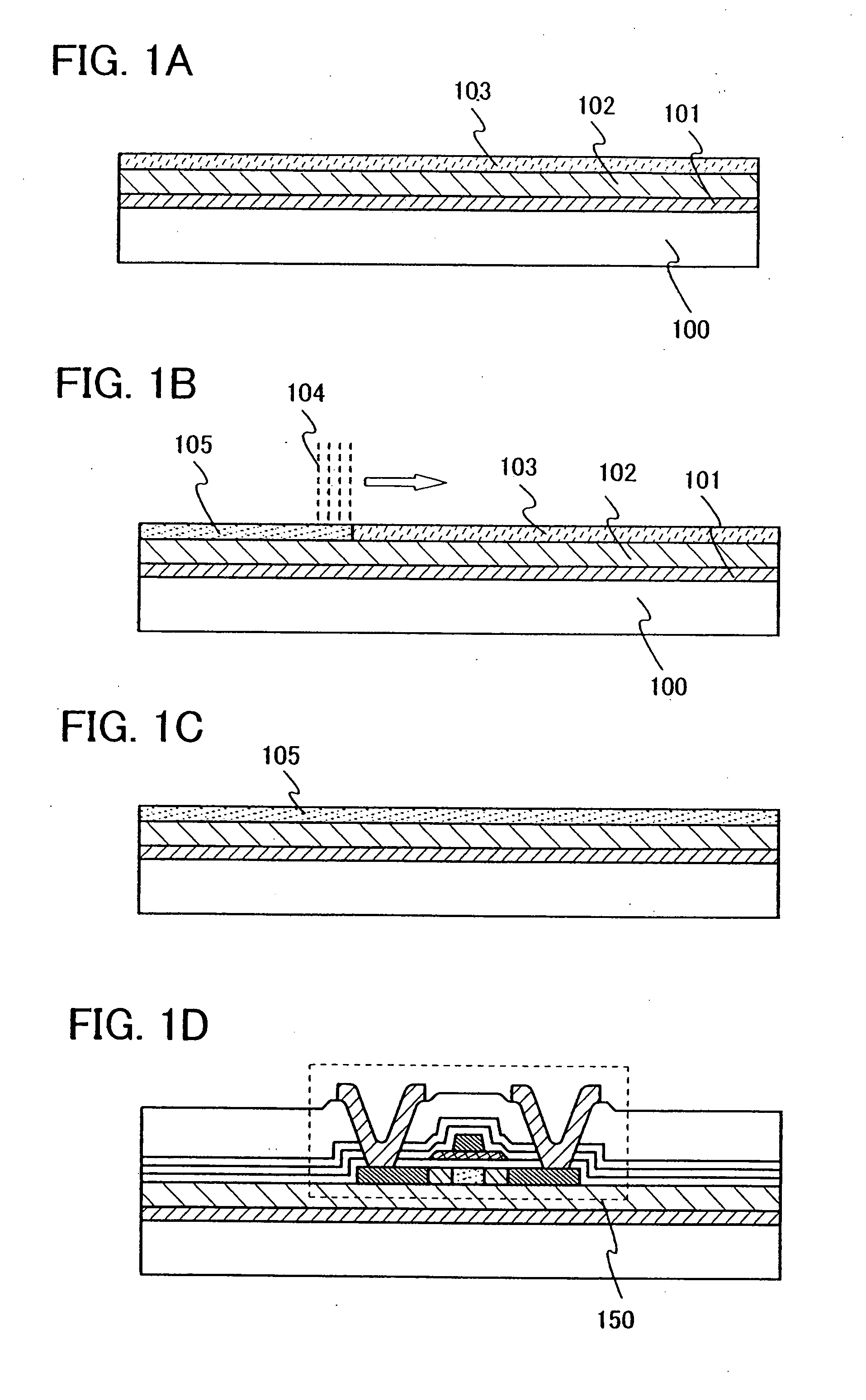
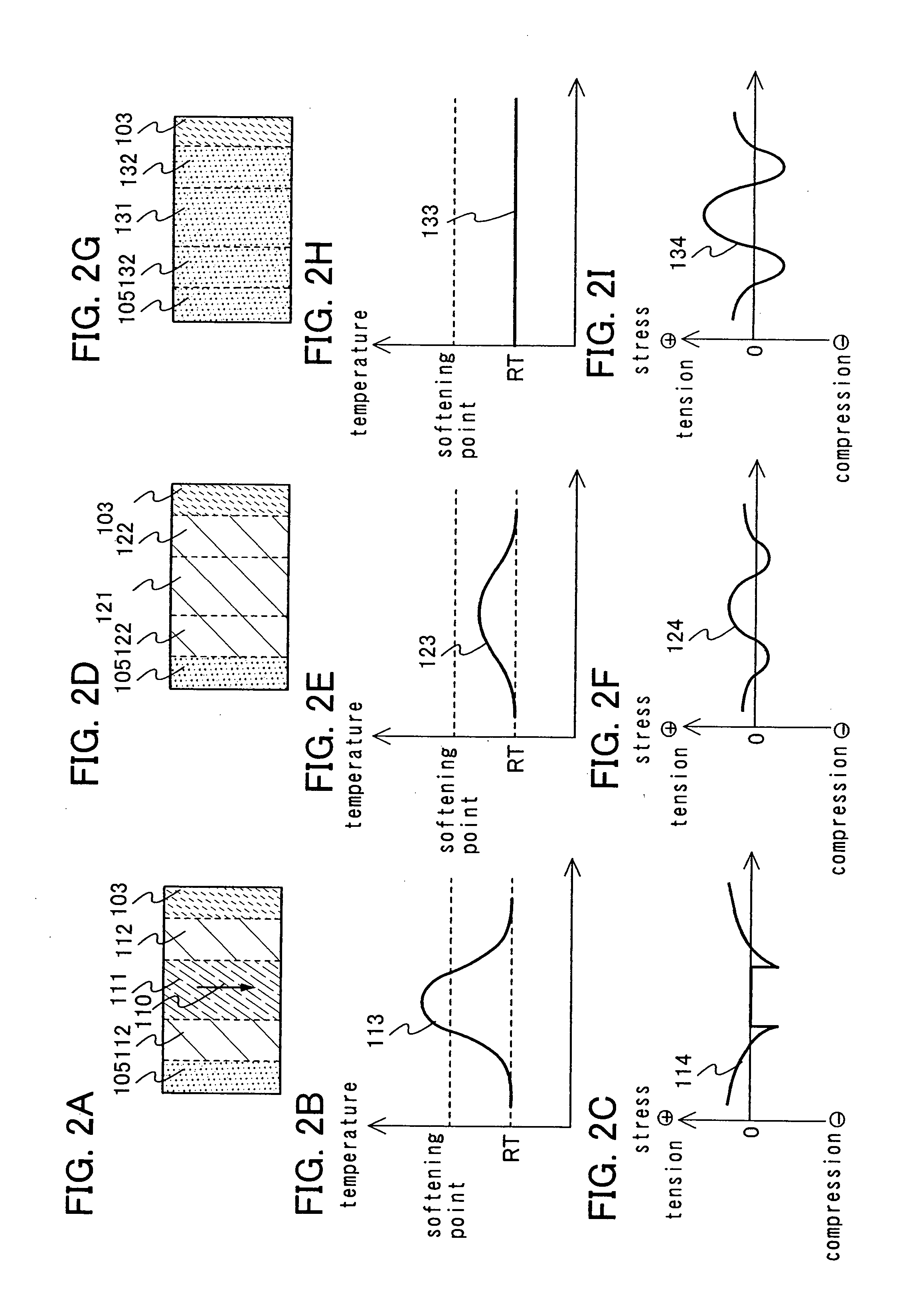
[0009]When the laser beam moves, the softened substrate surface also gradually cools and its volume contracts, so tensile stress occurs. Meanwhile, in the vicinity of the irradiation part of the laser beam, the heated substrate surface cools to room temperature. However, compressive stress remains. Due to the difference between the tensile stress and the compressive stress, a heat distortion remains in the substrate. If this heat distortion becomes larger than the rupture stress of the substrate, a crack forms in the substrate, and a crack also forms in the layer formed over the substrate surface. However, by forming a layer including a semiconductor film whose total stress after being heated is −500 N / m to +50 N / m, inclusive, preferably −150 N / m to 0 N / m, inclusive, over the substrate, the heat distortion which is generated in the substrate surface can be eased. As a result, the number of cracks in the substrate and the layer formed over the substrate can be reduced.
[0012]By forming a layer whose total stress after being heated is −500 N / m to +50 N / m, inclusive, preferably −150 N / m to 0 N / m, inclusive, over a substrate whose thermal expansion coefficient is greater than 6×10⁻⁷ / ° C. and less than or equal to 38×10−7 / ° C., preferably greater than 6×10⁻⁷ / ° C. and less than or equal to 31.8×10⁻⁷ / ° C., the formation of cracks in the substrate and the layer formed over the substrate when the layer formed over the substrate is irradiated with a continuous wave laser beam or a pulsed laser beam having a frequency of 10 MHz or more can be suppressed. That is, when the layer is irradiated with the laser beam, energy of the laser beam reaches the substrate, and in a part of the substrate having a thermal expansion coefficient of greater than 6×10⁻⁷ / ° C. and less than or equal to 38×10−7 / ° C., preferably greater than 6×10⁻⁷ / ° C. and less than or equal to 31.8×10⁻⁷ / ° C., a heat distortion is generated as a result of the heating by the laser beam irradiation and cooling. Due to the heat distortion, tensile stress is generated in a part of the substrate surface. However, since a layer having compressive stress is formed over the substrate, the tensile stress of the substrate surface can be eased. Therefore, the formation of cracks in the substrate and the layer can be suppressed. As a result, the number of defective semiconductor devices can be reduced, and yield can be improved.

Problems solved by technology

However, in a case where the above-described laser annealing method is used, there is a problem in that when the power of the laser beam is high, a crack may form in the substrate, the base protective film, or the crystalline silicon film.

Method used


Image

  • Method for manufacturing semiconductor device
  • Method for manufacturing semiconductor device
  • Method for manufacturing semiconductor device

Examples


embodiment mode 1

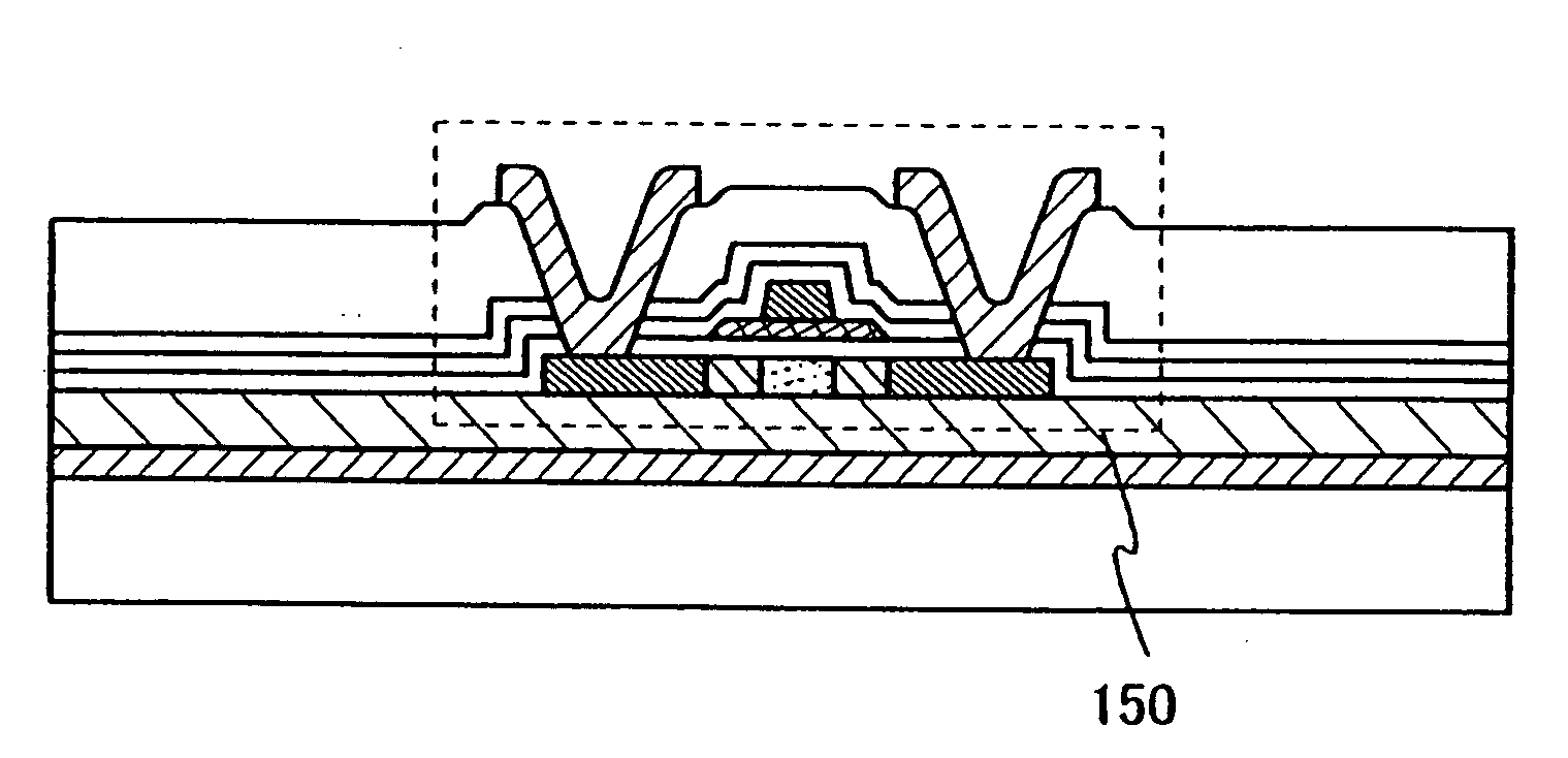
[0040]As shown in FIG. 1A, over one surface of a substrate 100 having an insulating surface, insulating films 101 and 102 which serve as base protective films are formed, and an amorphous semiconductor film 103 is formed over the insulating film 102. Next, in order to remove hydrogen of the amorphous semiconductor film, the amorphous semiconductor film is heated. At this time, the substrate and the insulating films which serve as base protective films are also heated. The insulating films 101 and 102 which serve as base protective films and the amorphous semiconductor film 103 are formed such that the total stress of the insulating films 101 and 102 and the amorphous semiconductor film 103 after the heating is −500 N / m to +50 N / m, inclusive, preferably −150 N / m to 0 N / m, inclusive.

[0041]As the substrate 100 having an insulating surface, a substrate which has a thermal expansion coefficient of greater than 6×10⁻⁷ / ° C. and less than or equal to 38×10−7 / ° C., preferably greater than 6×...

embodiment mode 2

[0087]In this embodiment mode, a liquid crystal display device which is an example of a semiconductor device will be described with reference to FIGS. 4A to 4D and FIGS. 5A to 5C.

[0088]As in Embodiment Mode 1, the insulating film 101 is formed over the substrate 100 which has a thermal expansion coefficient of greater than 6×10⁻⁷ / ° C. and less than or equal to 38×10−7 / ° C., preferably greater than 6×10⁻⁷ / ° C. and less than or equal to 31.8×10⁻⁷ / ° C., and the amorphous semiconductor film 103 is formed over the insulating film 101, as shown in FIG. 4A. Here, an AN100 substrate with a thermal expansion coefficient of 38×10−7 / ° C. and a thickness of 0.7 cm is used as the substrate 100. Further, as the insulating film 101, a silicon nitride film containing oxygen with a thickness of 40 to 60 nm and a silicon oxide film containing nitrogen with a thickness of 80 to 120 nm are each formed by a plasma CVD method. Further, as the amorphous semiconductor film 103, an amorphous semiconductor f...

embodiment mode 3

[0111]In this embodiment mode, a manufacturing process of a light emitting device having a light emitting element which is an example of a semiconductor device will be described.

[0112]As shown in FIG. 6A, the thin film transistors 225 to 227 are formed over the substrate 100 with the insulating film 101 therebetween using similar processing steps to those in Embodiment Mode 2. Further, the silicon oxide film 231, the silicon nitride film 232, and a silicon oxide film 233 are stacked as a first interlayer insulating film which insulates the gate electrodes and wirings of the thin film transistors 225 to 227. Further, wirings 308, 309, 310, 311, 312, and 313 which are connected to a semiconductor film of the thin film transistors 225 to 227, and a connecting terminal 314 are formed over the silicon oxide film 233, which is a part of the first interlayer insulating film.

[0113]Next, a second interlayer insulating film 315 is formed over the first interlayer insulating film, the wirings ...


PUM

PropertyMeasurementUnit
thicknessesaaaaaaaaaa

Abstract

It is an object to provide a method of manufacturing a crystalline silicon device and a semiconductor device in which formation of cracks in a substrate, a base protective film, and a crystalline silicon film can be suppressed. First, a layer including a semiconductor film is formed over a substrate, and is heated. A thermal expansion coefficient of the substrate is 6×10⁻⁷ / ° C. to 38×10−7 / ° C., preferably 6×10⁻⁷ / ° C. to 31.8×10⁻⁷ / ° C. Next, the layer including the semiconductor film is irradiated with a laser beam to crystallize the semiconductor film so as to form a crystalline semiconductor film. Total stress of the layer including the semiconductor film is −500 N / m to +50 N / m, preferably −150 N / m to 0 N / m after the heating step.

Description

BACKGROUND OF THE INVENTION[0001]1. Field of the Invention[0002]The present invention relates to a method for manufacturing a semiconductor device having a semiconductor element over a substrate with an insulating film therebetween.[0003]2. Description of the Related Art[0004]As a conventional method for manufacturing a polycrystalline semiconductor used for a thin film device such as an insulated-gate field-effect transistor, there is a method which employs a laser annealing method (for example, see Patent Document 1: Japanese Published Patent Application No. H 5-182923). Specifically, a silicon oxide film which is a base protective film is formed over a glass substrate, and an amorphous silicon film is formed over the silicon oxide film. Subsequently, heat annealing is performed to reduce the concentration of hydrogen contained in the amorphous silicon film, and a KrF excimer laser beam is irradiated onto the amorphous silicon film to crystallize the amorphous silicon film, thereb...

Claims


Application Information

Patent Timeline
Patent Type & Authority Applications(United States)
IPC IPC(8): H01L21/20
CPCH01L21/2026H01L27/1266H01L27/1285H01L27/1214H01L29/78603H01L21/02488H01L21/02422H01L21/02683H01L21/02532H01L21/02592H01L21/02686H01L21/02691H01L21/324H01L29/66757H01L29/78675
Inventor SHIMOMURA, AKIHISAMIYAIRI, HIDEKAZUISAKA, FUMITOJINBO, YASUHIROMARUYAMA, JUNYA
Owner SEMICON ENERGY LAB CO LTD
Learn More