Method for self-assembling microstructures

a microstructure and self-assembling technology, applied in the direction of microstructure device assembly, manufacturing tools, solventing apparatus, etc., can solve the problems of not meeting the design goal of the pick-and-place device, the electronic component quantity on the integrated circuit is relatively increased, and the electronic component size is required to be smaller

Inactive Publication Date: 2008-01-31
NAT TAIWAN UNIV
View PDF8 Cites 88 Cited by
  • Summary
  • Abstract
  • Description
  • Claims
  • Application Information

AI Technical Summary

Benefits of technology

[0015] The primary objective of the present invention is to provide a method for self-assembling micrometer or sub-micromet...

Problems solved by technology

However, as the need for minimization and multi-function of electronic products, the quantity of electronic components on the integrated circuit relatively increases and the size of the electronic components is required to be smaller.
However, when the size of the chip is smaller than 1 mm, the pick-and-place device is not going to fulfill the designed goal, even though these chips are attached by flip-chip method.
Vacuum, static or airflow etc. is introduced to hold the chip smaller than 1 mm, but because these chips are so small that the pick-and-place processing is too time consuming and cost ineffective.
Besides, the used equipment of above mentioned pick-and-place technique is very expensive, so it increases the difficulty and cost.
However, the high voltage required during the process to provide sufficient electrical field increases safety concerns and cost of manufacture so it is difficult to be used.
However, the low melting p...

Method used


Image

  • Method for self-assembling microstructures
  • Method for self-assembling microstructures
  • Method for self-assembling microstructures

Examples


Embodiment Construction

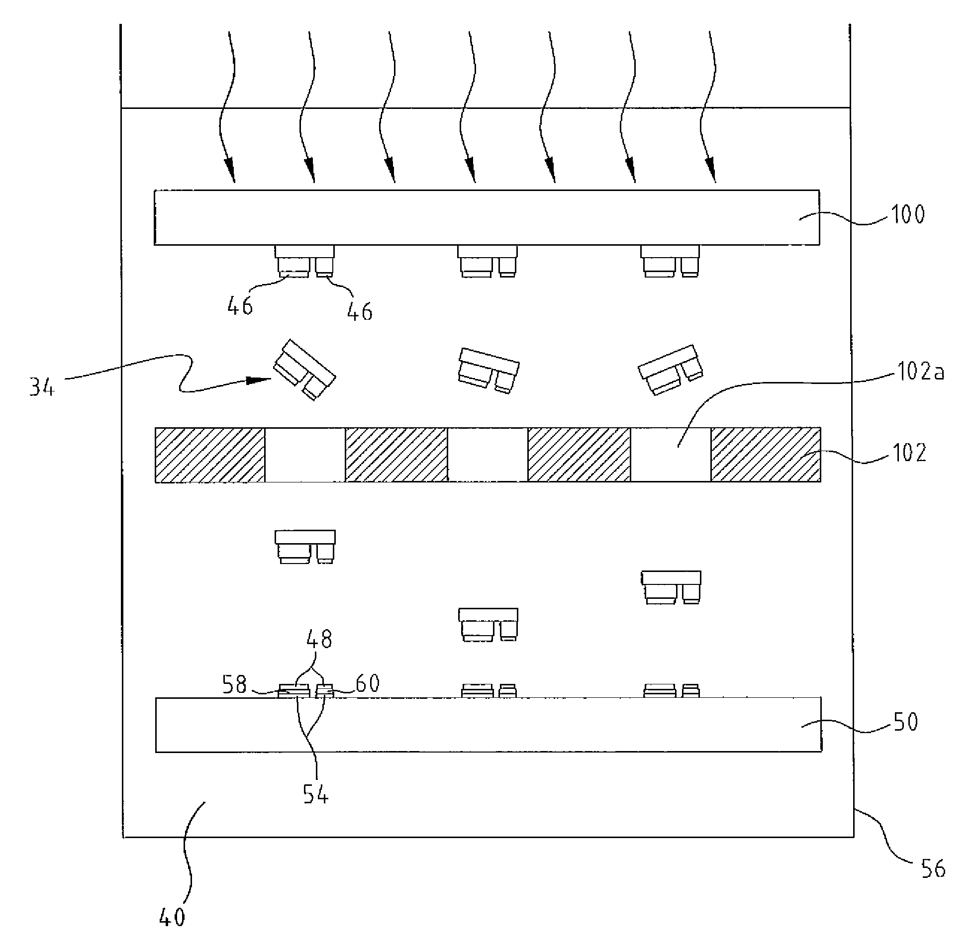
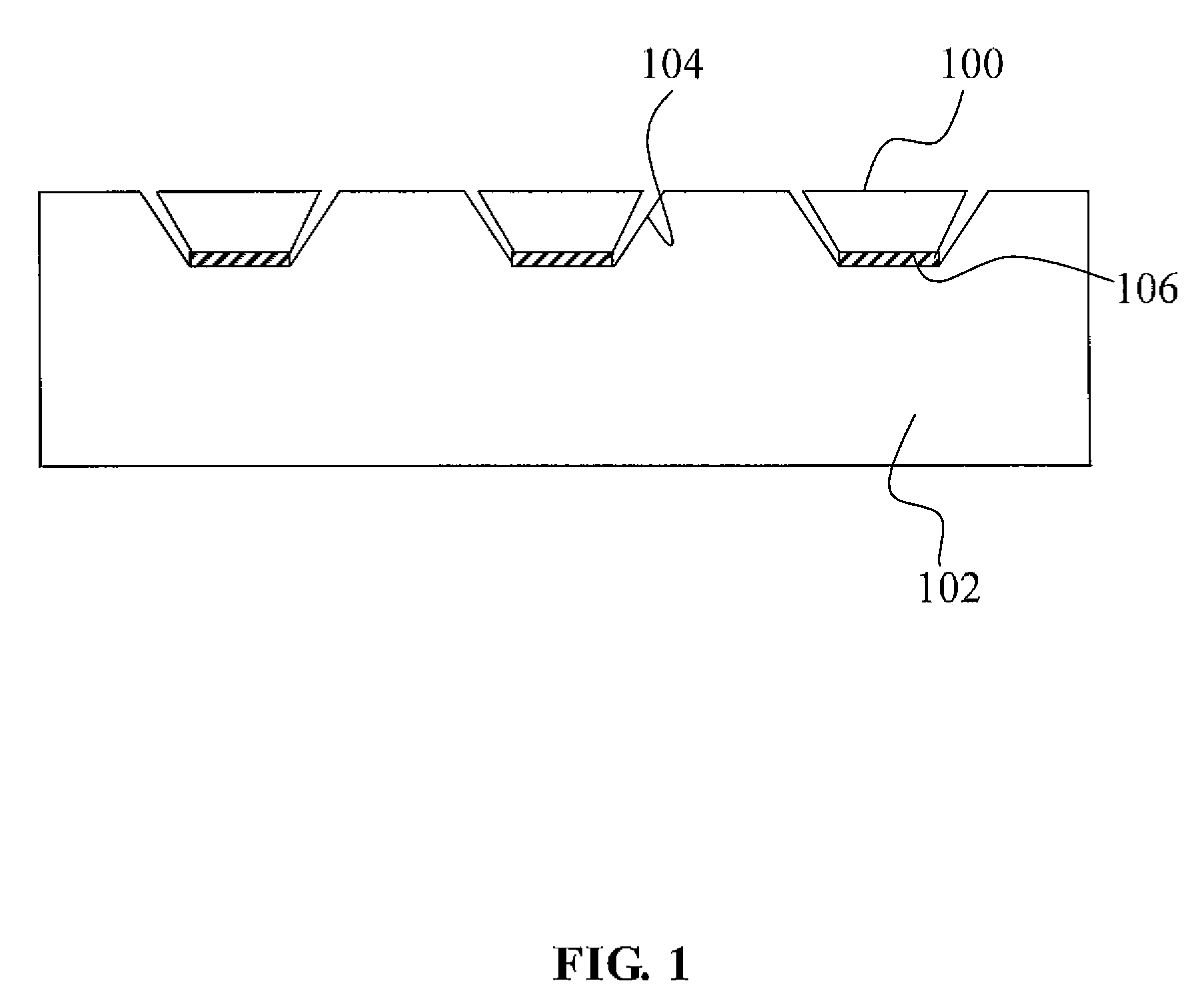
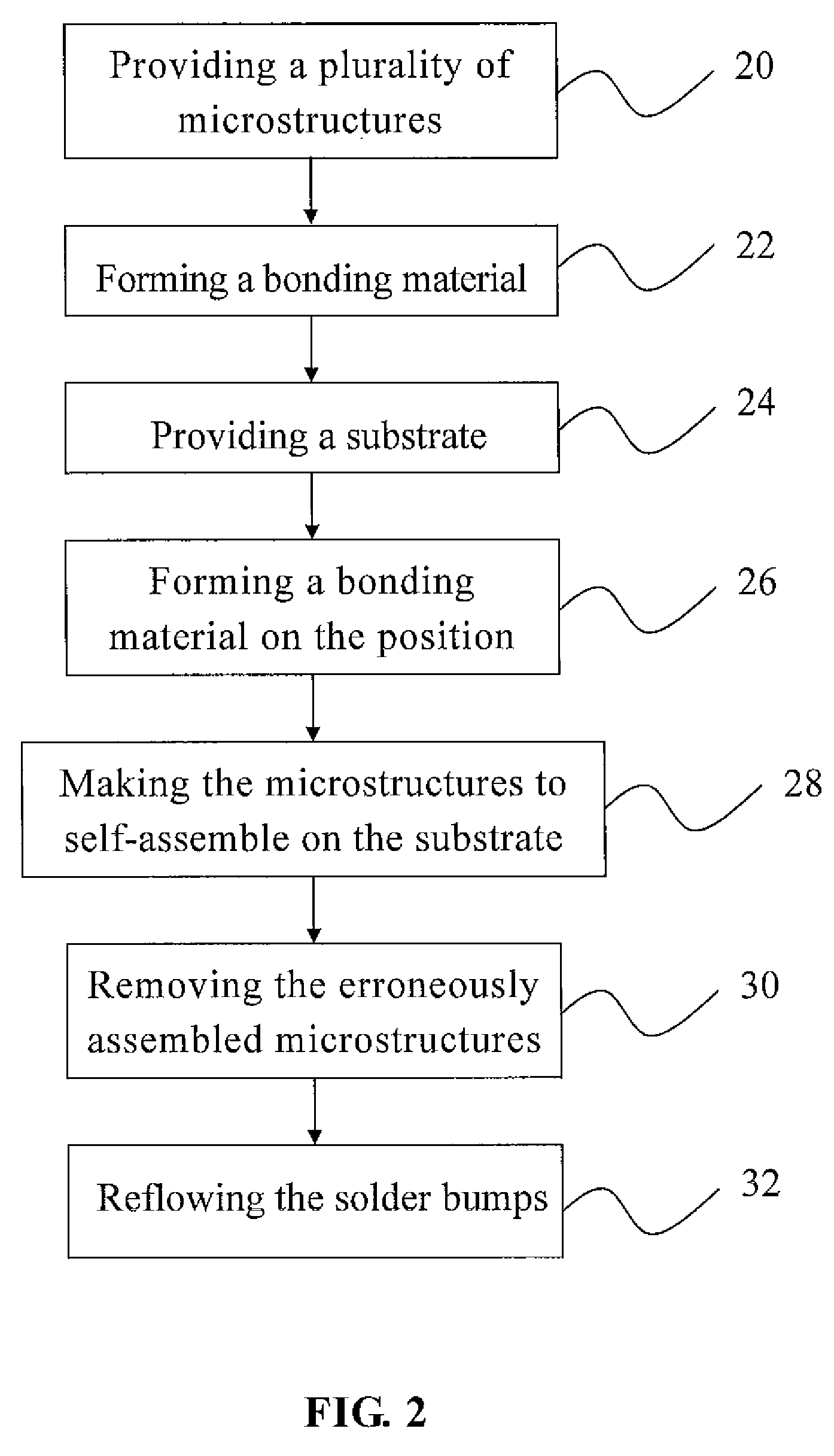
[0034] With reference to FIG. 2, it is noted that the flow chart of the method of the present invention is providing a plurality of microstructures 20 and forming a bonding material 22 on the surface of the microstructures, respectively. This method is providing a substrate 24, and forming a bonding material on the position 26 for bonding these microstructures onto the substrate. The bonding material used in the present invention may be any material that is able to physically attract to each other, e.g. interface force, field force, electrostatic force, electrophoresis effect etc. However, the examples are for illustrative purpose only and do not intend to limit the scope of the invention. The interface force may be hydrophilic or hydrophobic force but is not limited to the examples. The bonding material of the present invention includes self-assembly monolayers (SAMs), 2-ethyl-1-hexanol, flux, octanol or the equivalents. The field force of the present invention includes natural mag...


PUM

PropertyMeasurementUnit
Forceaaaaaaaaaa
Flexibilityaaaaaaaaaa
Microstructureaaaaaaaaaa

Abstract

A method for self-assembling a plurality of microstructures onto a substrate comprising using a bonding material to make the microstructure assembled onto the substrate by a physical attraction force The microstructures are self-aligned with the substrate, and further permanently fixed on and electrical connection with the substrate by the solder bumps between the microstructures and the substrate, which is formed by the solder bumps via reflow process. There is no need for the using of the conventional pick-and-place device in the present method. The present method could be applied to light emitting diodes, RFID tags, micro-integrated circuits or other types of microstructures.

Description

BACKGROUND OF THE INVENTION [0001] 1. Field of the Invention [0002] The present invention relates to a method for producing of electronic integrated circuit, and more particularly to a method for self-assembling chips onto a substrate. [0003] 2. Description of Related Art [0004] In general, an integrated circuit is composed of multiple electronic components on a single substrate so that the integrated circuit is high density and multi-functional. However, as the need for minimization and multi-function of electronic products, the quantity of electronic components on the integrated circuit relatively increases and the size of the electronic components is required to be smaller. [0005] Take a light emitting diode (LED), which is a component made by semiconductor material, as an example. In general, the LED is a miniature, solid type light-emitting source and is able to transform electrical energy into light. Because of its features of long life time, good shock-proof ability, low driv...

Claims


Application Information

Patent Timeline
IPC IPC(8): C23F1/00
CPCB23K3/0623H01L2224/95001B81C1/00214B81C3/002H01L24/95H01L25/50H01L2224/16H01L2224/95085H01L2224/95092H01L2224/95122H01L2924/01013H01L2924/01029H01L2924/01049H01L2924/01075H01L2924/01079H01L2924/01082H01L2924/10329H01L2924/14H01L2924/15153H01L2924/15155H01L2924/15165B23K2201/40H01L2924/01033H01L2924/01005H01L2924/01006H01L2924/12044H01L2924/12041H01L2224/05573H01L2224/05568H01L2924/00014H01L2224/95146H01L2224/0554B23K2101/40H01L2924/00H01L2224/05599H01L2224/0555H01L2224/0556
Inventor WU, ENBOACHANG, CHIAN-SHOU
Owner NAT TAIWAN UNIV
Why Eureka
Try Eureka