

Laminated structure, production method of the same, multilayer circuit board, active matrix substrate, and electronic display
a technology of active matrix substrate and laminated structure, which is applied in the direction of layered products, transportation and packaging, coatings, etc., can solve the problems of degrading the quality of transistors, difficult to form fine conductive patterns (or wiring) constituting transistors of active matrix substrates, and difficult to form fine functional material patterns. , to achieve the effect of high surface energy, low surface energy, and high surface energy
- Summary
- Abstract
- Description
- Claims
- Application Information
AI Technical Summary
Benefits of technology
Problems solved by technology
Method used
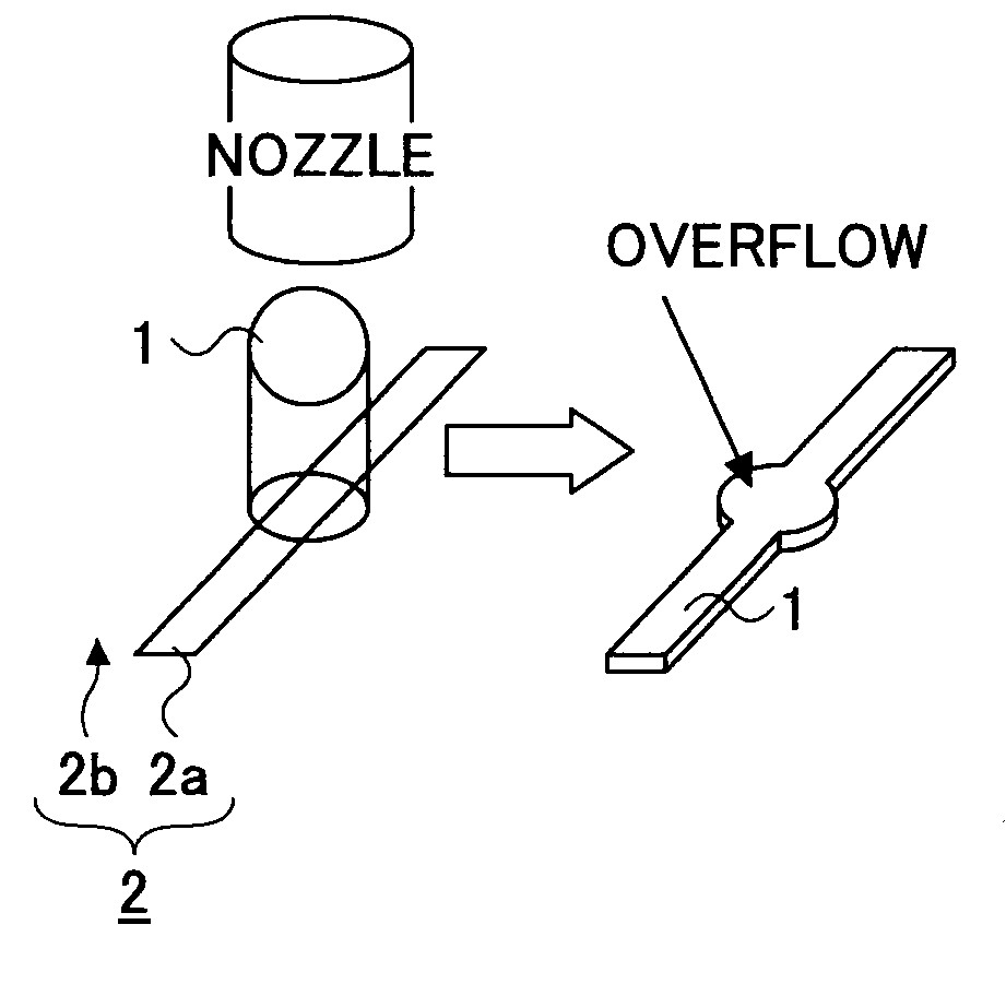
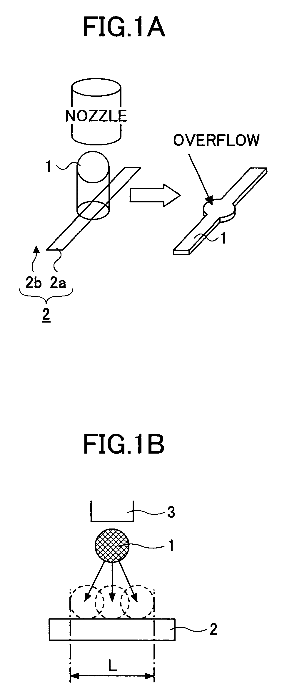
Image

Examples
example 1
[0120]In example 1, flow of the functional fluid 60 was observed through the experiments described below.
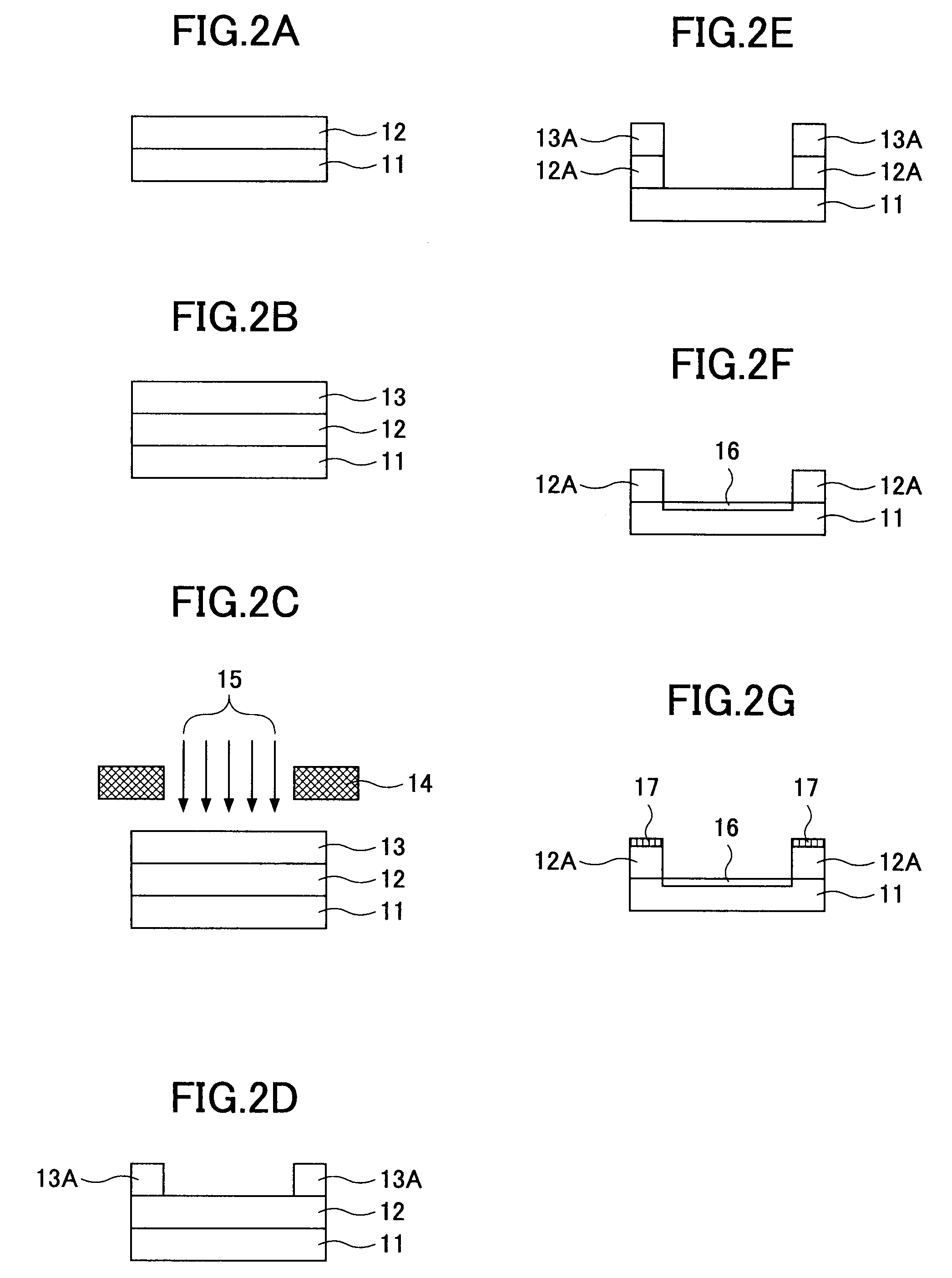
[0121]First, an NMP solution containing a wettability-variable material was applied to a glass substrate by spin-coating. As the wettability-variable material, a polyimide material having an alkyl group in its side chain was used, the surface free energy of which polyimide material changes when irradiated by ultraviolet light. Next, the NMP solution was pre-calcined in an oven at 100° C. and then calcined at 180° C. to remove the solvent and thereby to form the wettability-variable layer 30 (see FIGS. 6A and 6B).
[0122]A portion of the wettability-variable layer 30 was exposed to ultraviolet light with a wavelength of 300 nm or smaller (using an ultra-high pressure mercury lamp) through a photomask having a certain pattern to form a corresponding pattern comprising the high-surface-energy area 40 and the low-surface-energy area 50 on the wettability-variable layer 30. The high-sur...
example 2
[0130]In example 2, the width W1 of the first area 40a and the width W2 of the second area 40b were set as shown in table 1 and wettability-variable layers 30A through 30E having different characteristics were used to observe the flow of the functional fluid 60. Other conditions and the method of experiments in example 2 were substantially the same as those of example 1. Table 1 shows the widths W1 of the first area 40a, the widths W2 of the second area 40b, and corresponding results of the experiments for each of the wettability-variable layers 30A through 30E.
TABLE 1Wettability-variableWidth W1 (μm) ofWidth W2 (μm) ofW1 / layers 30first area 40asecond area 40bW2ABCDE80501.6⊚⊚X⊚⊚120502.4⊚⊚X⊚⊚80302.7⊚⊚X⊚⊚120304.0⊚◯X⊚⊚200504.0⊚◯X⊚⊚200306.7⊚ΔX◯⊚80108.0⊚ΔXΔ⊚1201012.0◯ΔXΔ⊚2001020.0ΔΔXΔ⊚⊚: The conductive layer 70 was successfully formed on the entire high-surface-energy area 40.◯: Breaks were observed in some cases in the conductive layer 70 on the second area 40b.Δ: Breaks were observed i...
example 3
[0139]In example 3, a multilayer circuit board was prepared by forming a source electrode 232 and a source signal line 292 using the conductive layer 70 described above.
[0140]FIG. 15A shows a top view of a multilayer circuit board of comparative example 1, FIG. 15B shows a top view of a multilayer circuit board of example 3, and FIG. 15C is a cross-sectional view taken along line A-A of the multilayer circuit board shown in FIG. 15A or 15B. On each of the multilayer circuit boards, a drain electrode 242 was formed in addition to the source electrode 232 and the source signal line 292.
[0141]For descriptive purposes, FIGS. 15A and 15B each shows only a portion of a multilayer circuit board which portion corresponds to one pixel. It is assumed that 1000 pixels are arranged in a line on each of the multilayer circuit boards of comparative example 1 and example 3. The size of each pixel is 317.5 μm that corresponds to 80 ppi. The wettability-variable material (polyimide material), the fu...
PUM
 Abstract
Description
Claims
Application Information