Solid state imaging device, method for fabricating the same, and camera

a technology of solid-state imaging and manufacturing methods, which is applied in the direction of diodes, semiconductor devices, radio-controlled devices, etc., can solve the problems of deterioration of noise characteristics, solid-state imaging devices, and preventing the achievement of high-performance solid-state imaging devices, so as to secure the electrical isolation characteristics of the device isolation region and increase the number of electrons accumulating in the photoelectric conversion portion

Active Publication Date: 2008-02-07
GK BRIDGE 1
View PDF9 Cites 19 Cited by
  • Summary
  • Abstract
  • Description
  • Claims
  • Application Information

AI Technical Summary

Benefits of technology

[0051]As described above, the present invention can provide the following solid state imaging device and the method for fabricating the same. The solid state imaging device secures the electrical isolation characteristics of a device isolation region. At the same time, even with miniaturization in the pixel size, the amount of dark current and the number of white blemishes both determining the characteristics of a photoelectric conversion portion of the solid state imaging device are small, and the number of electrons accumulable in the photoelectric conversion portion increases.

Problems solved by technology

In this etching, the amount of unnecessary electric charges produced even under dark conditions on which the silicon substrate is not irradiated with light increases due to etching damage, resulting in a deterioration in noise characteristics.
However, the solid state imaging device of the known example has problems that will be described below.
This prevents a high-performance solid state imaging device from being achieved.
Furthermore, since lithography needs to be carried out twice, the TAT (turn around time) is increased, resulting in increased cost.

Method used


Image

  • Solid state imaging device, method for fabricating the same, and camera
  • Solid state imaging device, method for fabricating the same, and camera
  • Solid state imaging device, method for fabricating the same, and camera

Examples


embodiment

[0065]A solid state imaging device according to an embodiment of the present invention will be described hereinafter with reference to the drawings.

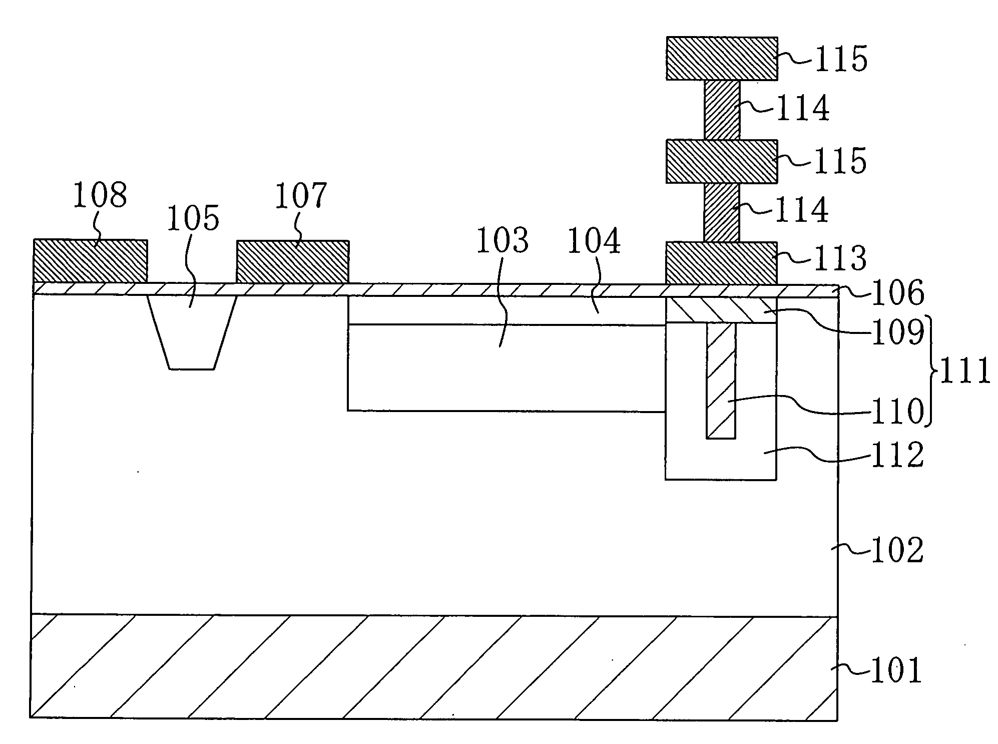
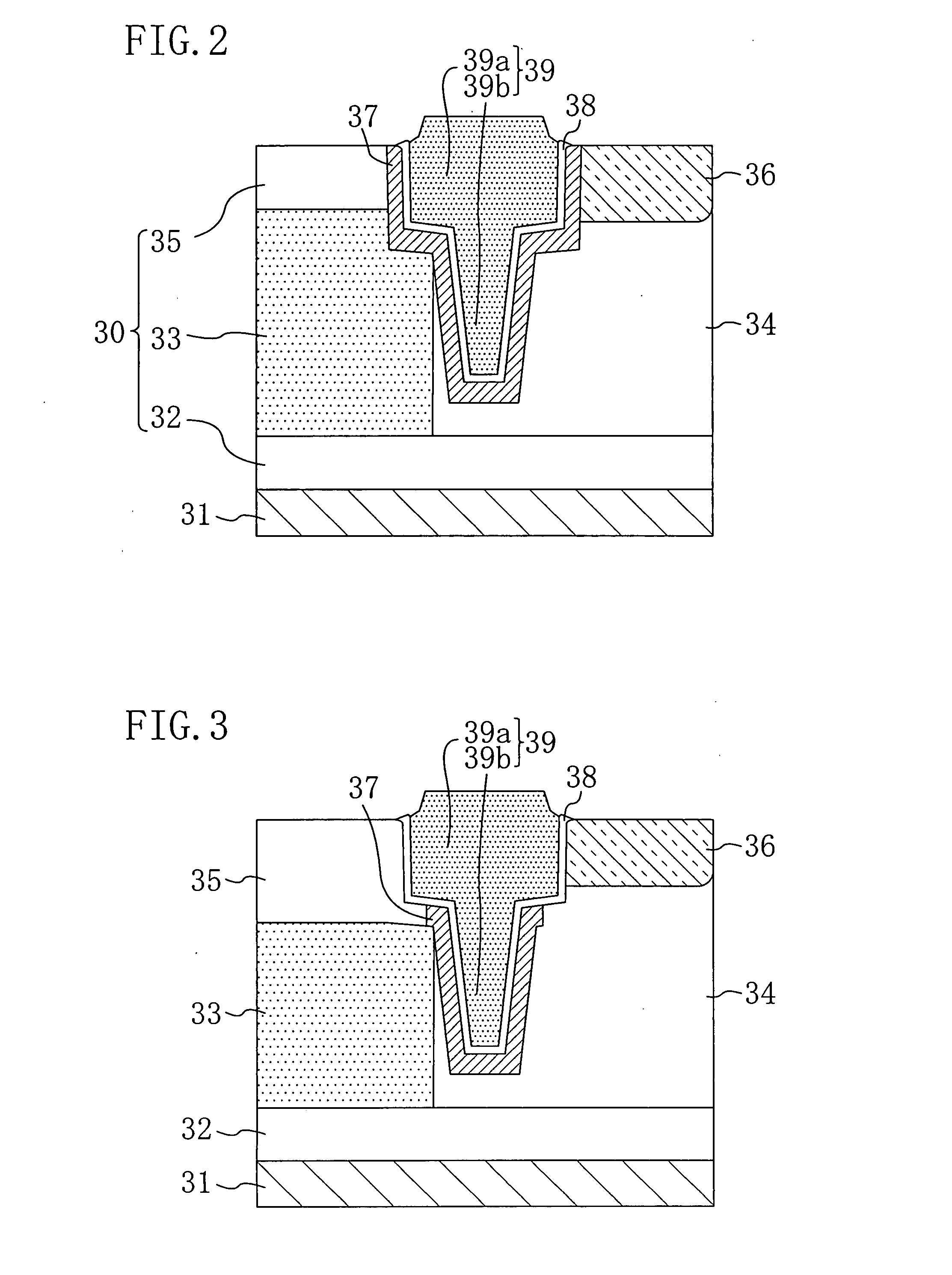
[0066]FIG. 2 illustrates a cross-sectional structure of a part of the solid state imaging device including a photodiode and an active region according to the embodiment of the present invention. Interconnects and interlayer films formed on a semiconductor substrate are not shown. FIGS. 3 through 5 that will be described below illustrate modifications of the embodiment of the present invention. Like FIG. 2, these figures each illustrate a cross-sectional structure of a part of a solid state imaging device including a photodiode and an active region.

[0067]As illustrated in FIG. 2, a photodiode 30 serving as a photoelectric conversion portion of the solid state imaging device has a P+NP− structure in the top surface of the silicon substrate 31. The P+NP− structure includes a P+ surface layer (a region of the silicon substrate 31 in which da...


PUM


Abstract

A solid state imaging device includes: an imaging region formed in an upper part of a substrate made of silicon to have a photoelectric conversion portion, a charge accumulation region of the photoelectric conversion portion being of a first conductivity type; a device isolation region formed in at least a part of the substrate to surround the photoelectric conversion portion; and a MOS transistor formed on a part of the imaging region electrically isolated from the photoelectric conversion region by the device isolation region. The width of the device isolation region is smaller in its lower part than in its upper part, and the solid state imaging device further includes a dark current suppression region surrounding the device isolation region and being of a second conductivity type opposite to the first conductivity type.

Description

BACKGROUND OF THE INVENTION[0001](1) Field of the Invention[0002]The present invention relates to solid state imaging devices each including an imaging region which has a plurality of pixels over a semiconductor substrate, methods for fabricating the same, and cameras.[0003](2) Description of Related Art[0004]A MOS (Metal Oxide Semiconductor) solid state imaging device is an image sensor in which a signal accumulated in a photodiode forming a corresponding pixel is read by an amplification circuit including a MOS transistor. Such a MOS solid state imaging device is advantageously capable of low voltage operation and high-speed charge reading and can be integrated with peripheral circuits into one chip.[0005]In view of the above, attention has been paid to MOS solid state imaging devices as imaging devices used for digital cameras and portable devices, such as mobile phones. In recent years, particularly, for the MOS solid state imaging devices, reduction in cell size and improvement...

Claims


Application Information

Patent Timeline
Patent Type & Authority Applications(United States)
IPC IPC(8): H01L31/113H01L21/265H01L21/76H01L27/146
CPCH01L27/1463H01L27/14683H01L27/14643
Inventor MORI, MITSUYOSHIYAMAGUCHI, TAKUMIOKINO, TORU
Owner GK BRIDGE 1
Why Eureka
Try Eureka