Solder Interconnect Joints For A Semiconductor Package

a technology of interconnect joints and semiconductors, applied in the direction of soldering apparatus, sustainable manufacturing/processing, final product manufacturing, etc., can solve the problems of increasing damage, local contamination of solder, and poor fatigue life of solder interconnects, so as to reduce damage, constrain crack propagation, and increase the fatigue life of solder joints

Inactive Publication Date: 2008-02-07
IBM CORP
View PDF5 Cites 18 Cited by
  • Summary
  • Abstract
  • Description
  • Claims
  • Application Information

AI Technical Summary

Benefits of technology

[0014] It is another object of the invention to produce a solder joint that constrains cracking along the intermetallic boundary.
[0015] In accordance with the present invention, there is provided a method and article of fabrication, featuring a solder layer that comprises a serpentine, interrupted, or interdigitated boundary. The non-planar design of the boundary layer increases the fatigue life of the solder joint, by limiting the damage caused by micro-cracking. This irregularity of the solder boundary constrains the propagation of cracks by creating obstacles along the crack path, redirecting the crack away from the intermetallic layer, or by increasing the path length along which the crack propagates. The present invention seeks to increase the fatigue life of the solder joint, by limiting the damage caused by micro-cracking in the solder joint. This objective is achieved by redistributing the stresses in solder, thus constraining the cracks. Such containment can be accomplished by creating obstacles along the crack path, redirecting the crack away from the intermetallic layer, or by increasing the path length along which the crack is to propagate. The solder layer can be designed to include a serpentine, interrupted, or interdigitated boundary. The method can be applied to ball grid arrays, column grid arrays, surface mount technology (SMT) joints, etc.

Problems solved by technology

The fatigue life of solder interconnects is often poor, because cracks develop near an intermetallic layer.
The damaging process is due to the build-up of inelastic deformation (creep) that leads to cavity nucleation, growth, and coalescence along grain boundaries.
The increasing damage tends to produce micro-cracks at the boundaries.
It is also observed that dissolved copper, gold, or other metallic pad coating materials locally contaminate solder.
The contaminants increase the solder brittleness, making the solder susceptible to micro-cracking, when compared with bulk behavior.

Method used


Image

  • Solder Interconnect Joints For A Semiconductor Package
  • Solder Interconnect Joints For A Semiconductor Package
  • Solder Interconnect Joints For A Semiconductor Package

Examples


Embodiment Construction

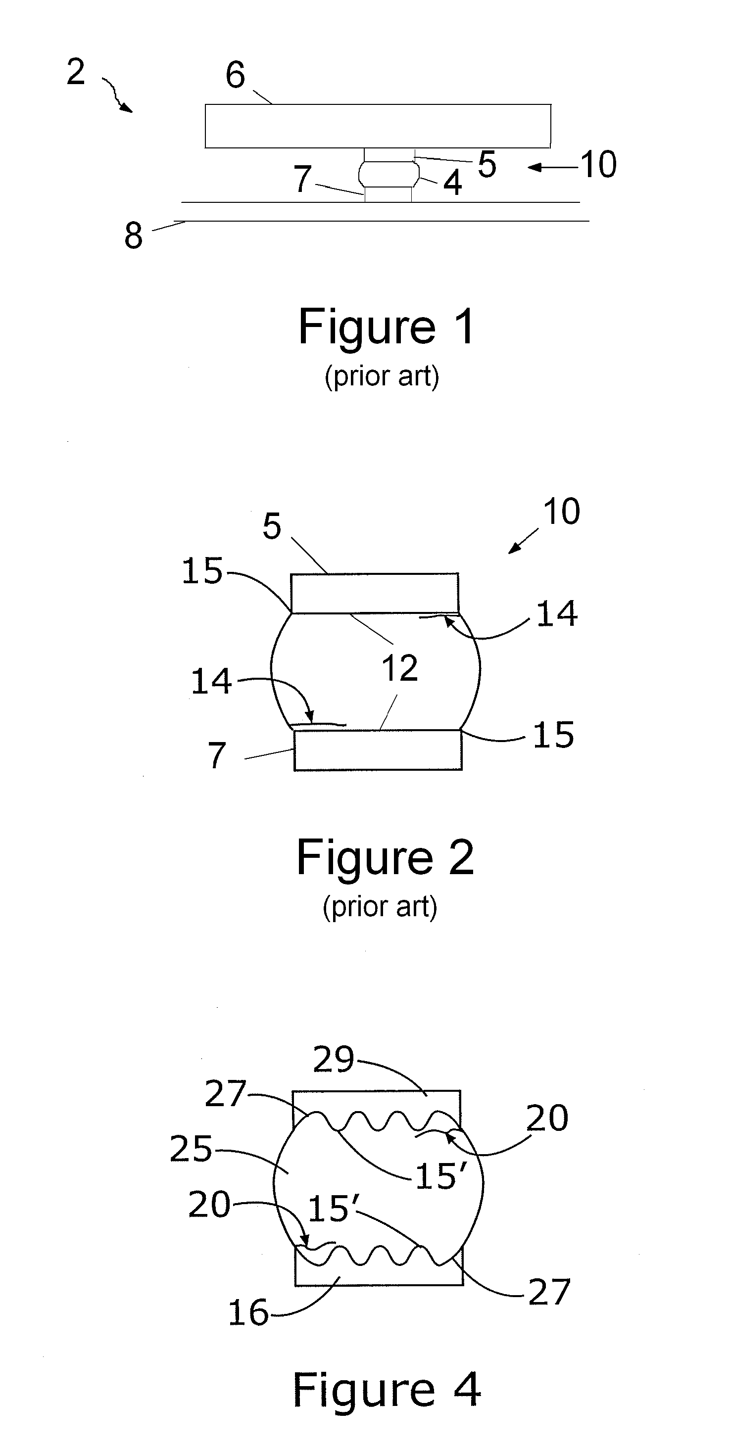
[0022] Referring now to the drawings, wherein like reference numerals refer to like parts throughout, there is seen in FIG. 1 a conventional electronic package 2 including a solder joint 10 interconnecting a semiconductor 6, such as an integrated chip, to a substrate 8, such as a printed circuit board. Solder joint 10 generally comprises a solder ball 4 interconnected to a metal pad 5 of semiconductor 6 and also interconnected to a metal pad 7 of substrate 8, thereby electrically interconnecting semiconductor 6 to substrate 8. It should be recognized by those of ordinary skill in the art that the present invention is directed to applications such as ball grid arrays, column grid arrays, and surface mount technology (SMT), all of which are well known forms of geometry used for mounting semiconductor chips to substrates and forming semiconductor packages.

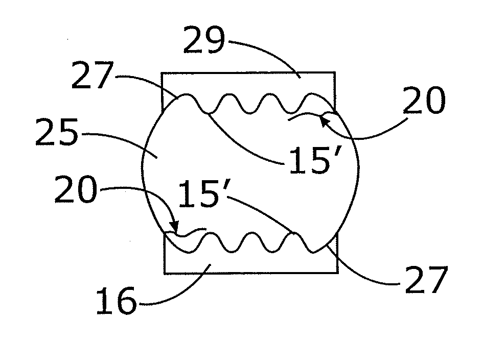
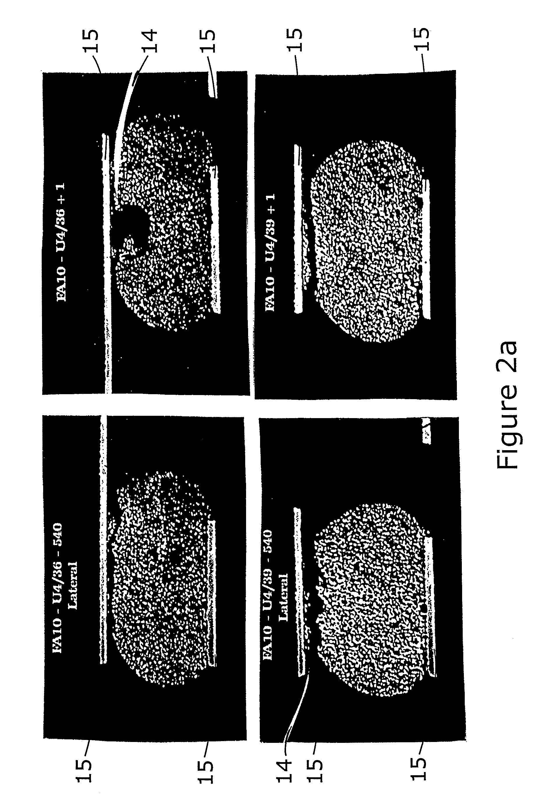
[0023] As seen in FIG. 2, in a conventional solder joint 10 micro-cracks 14 are free to propagate in solder joint 10 near the junct...


PUM

PropertyMeasurementUnit
grain boundariesaaaaaaaaaa
tensile stressaaaaaaaaaa
stress concentrationaaaaaaaaaa

Abstract

A method and article of fabrication is described featuring a solder layer having a serpentine, interrupted, or interdigitated boundary. The non-planar design of the boundary layer increases the fatigue life of the solder joint by limiting the damage caused by micro-cracking. This irregularity of the solder boundary constrains the propagation of cracks by creating obstacles along the crack path, redirecting the crack away from the intermetallic layer, or by increasing the path along which the crack propagates.

Description

CROSS-REFERENCE TO RELATED APPLICATIONS [0001] This application is a continuation-in-part of U.S. patent application Ser. No. 10 / 038,264, filed Jan. 3, 2002, which is a divisional of U.S. patent application Ser. No. 09 / 430,965, filed Nov. 1, 1999.BACKGROUND OF THE INVENTION [0002] 1. Field of the Invention [0003] The present invention relates to soldering techniques and, more particularly, to a solder method that enhances solder interconnects by eliminating solder joint failures in semiconductor packages that are caused by micro-cracking at or near the solder intermetallic interface between the semiconductor pad and substrate pad. [0004] 2. Description of the Related Art [0005] The fatigue life of solder interconnects is often poor, because cracks develop near an intermetallic layer. The damaging process is due to the build-up of inelastic deformation (creep) that leads to cavity nucleation, growth, and coalescence along grain boundaries. The increasing damage tends to produce micro...

Claims


Application Information

Patent Timeline
Patent Type & Authority Applications(United States)
IPC IPC(8): H01L23/488B23K3/06B23K35/02B23K35/14H01L21/48H01L21/60H01L23/485H01L23/498H05K1/11H05K3/34
CPCB23K3/06H01L2924/01033B23K35/0233H01L21/4853H01L23/49816H01L24/02H01L24/11H01L24/12H01L2224/0401H01L2224/13099H01L2924/01005H01L2924/01006H01L2924/01013H01L2924/01029H01L2924/01079H01L2924/01327H01L2924/014H01L2924/14H05K1/111H05K3/3436H05K2201/0373H05K2203/0405B23K35/0222H01L2224/05557H01L2224/05552H01L24/05H01L24/13H01L24/16Y02P70/50
Inventor PARK, SEUNGBAESATHE, SANJEEVZUBELEWICZ, ALEKSANDER
Owner IBM CORP
Why Eureka
Try Eureka