Power Semiconductor Devices Having Integrated Inductor

a technology of integrated inductors and power semiconductors, applied in the direction of transformers/inductance details, inductances, basic electric elements, etc., can solve the problems of excessive resistance loss, thermal heating, and unwelcome roadblocks to miniaturization, so as to improve the performance of thermal devices and reduce the time to market

Active Publication Date: 2008-02-07
TEXAS INSTR INC
View PDF1 Cites 49 Cited by
  • Summary
  • Abstract
  • Description
  • Claims
  • Application Information

AI Technical Summary

Benefits of technology

[0005]Applicant recognizes the need for a fresh approach to integrate the inductor with the circuit and to offer at the same time the opportunity to fine-tune the inductance characteristics, improve the thermal device performance, and shield the magnetic field from interfering with the circuit. The methodology should be coherent, low-cost, and flexible e

Problems solved by technology

However, an unwelcome roadblock to miniaturization appears, whenever a component has to be added as a discrete external part to the product, rather than to be integrated into already existing devices.
The addition of an external part is particularly bothersome in power driver circuits, DC-to-DC converter

Method used


Image

  • Power Semiconductor Devices Having Integrated Inductor
  • Power Semiconductor Devices Having Integrated Inductor
  • Power Semiconductor Devices Having Integrated Inductor

Examples


Embodiment Construction

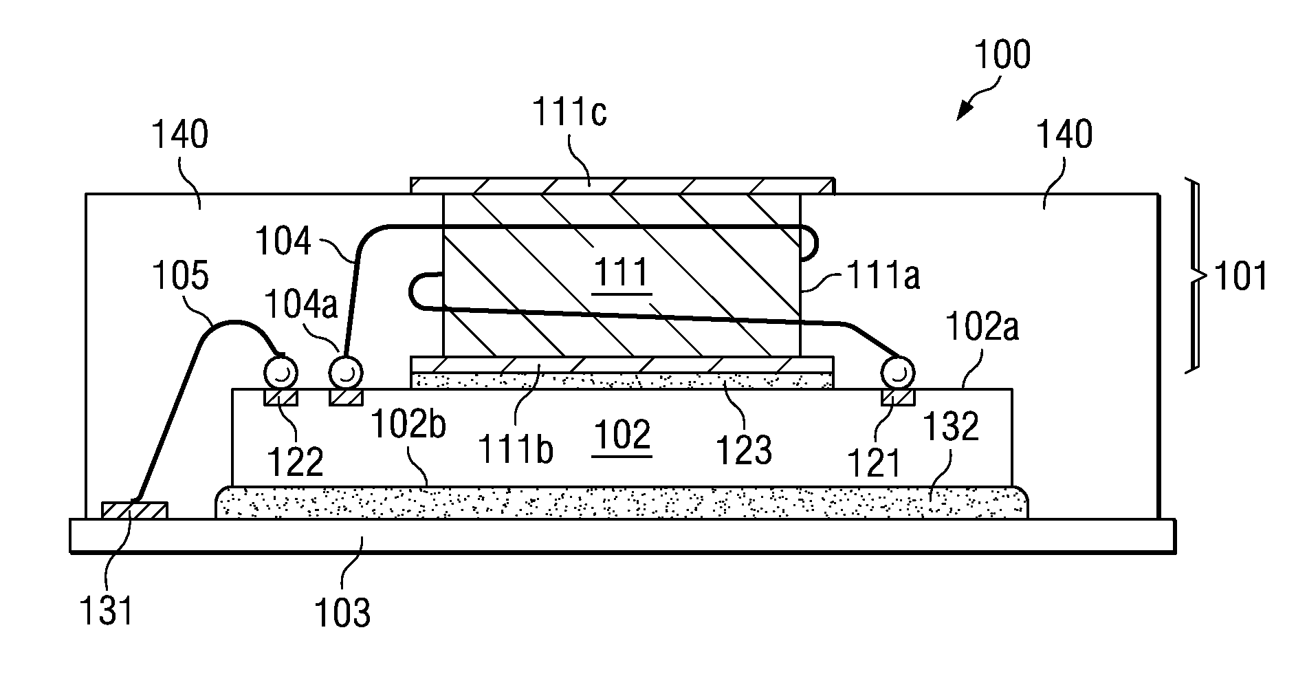
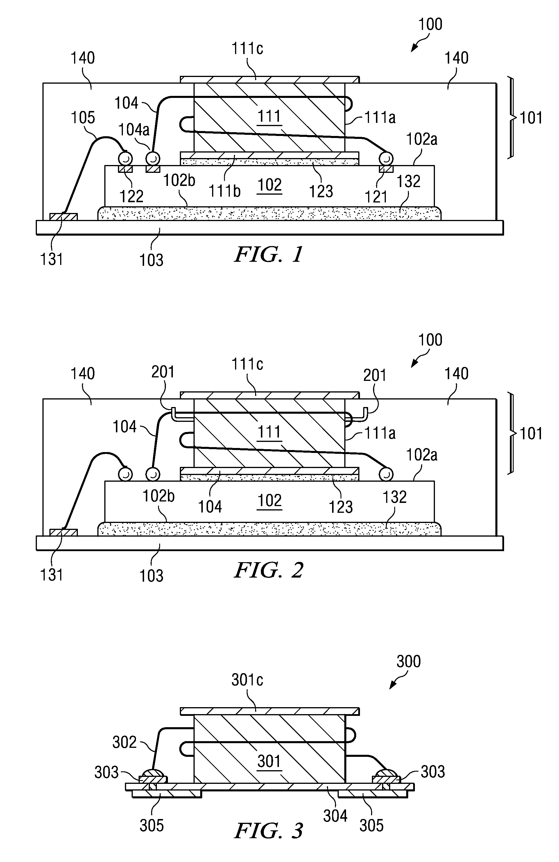
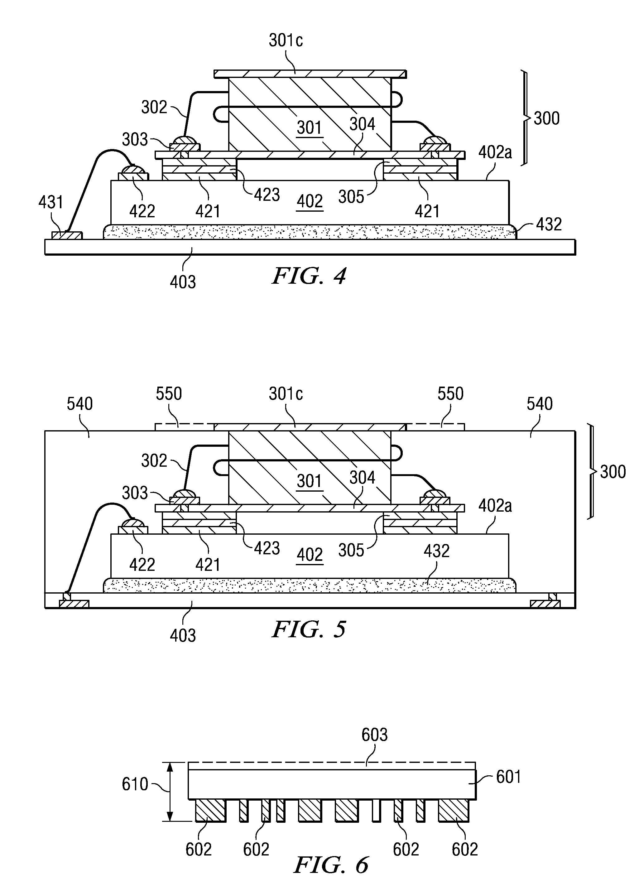
[0027]FIG. 1 illustrates an embodiment, generally designated 100, which integrates an inductor, capable of generating an inductance of several hundred nano-Henry (nH), with a semiconductor power component, such as a power driver circuit, a DC-to-DC converter, or a power controller circuit. The inductor 101 is positioned on top of the chip or component 102, which in turn is assembled on a substrate 103.

[0028]Component 102 may be an integrated circuit chip, a discrete component, or a multi-chip arrangement; it may include semiconductor devices made of silicon, silicon germanium, gallium arsenide, or any other semiconductor material. Component 102 has a certain area, and an active surface 102a and a passive surface 102b. On the active surface 102a are a first set of terminals 121 and a second set of terminals 122.

[0029]Inductor 101 has a body 111, which includes ferromagnetic material such as iron. The body has a periphery 111a and a flat surface 111b. The flat surface 111b has an area...


PUM


Abstract

An electronic device (100) with one or more semiconductor chips (102) has an inductor (101) assembled on or under the chips. The inductor includes a ferromagnetic body (111) and a wire (104) wrapped around the body to form at least a portion of a loop; the wire ends (104a) are connected to the chips. The assembly is attached to a substrate (103), which may be a leadframe. The device may be encapsulated in molding compound (140) so that the inductor can double as a heat spreader (111c), enhancing the thermal device characteristics.

Description

FIELD OF THE INVENTION[0001]The present invention is related in general to the field of semiconductor devices and processes, and more specifically to structure and method of integrated inductors for power semiconductor devices.DESCRIPTION OF THE RELATED ART[0002]Time to Market is a significant factor for the success of semiconductor components in the rapidly expanding markets served by electronic products. All too often, though, a redesign of the semiconductor component is required in order to satisfy the changing characteristic requested by a customer or by the technical needs of a new trend in products.[0003]Another significant success factor for semiconductor products is the capability to satisfy the market trend for miniaturization. This trend is driven and accelerated by new applications for semiconductor products such as hand-held appliances, which prefer small-size components. However, an unwelcome roadblock to miniaturization appears, whenever a component has to be added as ...

Claims


Application Information

Patent Timeline
IPC IPC(8): H01L23/52H01L23/48H01L29/40
CPCH01F17/045H01L2924/01033H01F27/40H01L23/3121H01L23/495H01L23/49575H01L23/645H01L24/16H01L24/17H01L24/29H01L24/33H01L24/45H01L24/48H01L24/49H01L24/85H01L25/16H01L2224/13099H01L2224/32225H01L2224/32245H01L2224/45144H01L2224/45147H01L2224/4809H01L2224/48091H01L2224/4813H01L2224/48137H01L2224/48227H01L2224/48235H01L2224/48247H01L2224/48464H01L2224/48465H01L2224/48472H01L2224/48599H01L2224/49H01L2224/73253H01L2224/73265H01L2224/85H01L2924/01014H01L2924/01028H01L2924/01029H01L2924/01031H01L2924/01032H01L2924/01046H01L2924/01047H01L2924/01078H01L2924/01079H01L2924/01082H01L2924/014H01L2924/078H01L2924/12044H01L2924/14H01L2924/19041H01L2924/19042H01L2924/19104H01L2924/19107H01L2924/30107H01L2924/3025H01F27/027H01L2924/01006H01L2924/00014H01L2224/78H01L2924/00H01L2924/00012H01L2224/45015H01L2924/181H01L2224/48092H01L24/73
Inventor KODURI, SREENIVASAN K.
Owner TEXAS INSTR INC
Why Eureka
Try Eureka