

Semiconductor integrated circuit device and receiving device
a technology of integrated circuit and integrated circuit device, which is applied in the direction of burglar alarm mechanical actuation, burglar alarm by hand-portable object removal, instruments, etc., can solve the problems of inconvenient radio transmitter, long processing time, and inability to respond in tim
- Summary
- Abstract
- Description
- Claims
- Application Information
AI Technical Summary
Benefits of technology
Problems solved by technology
Method used
Image

Examples
embodiment 1
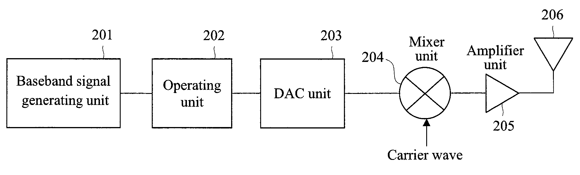
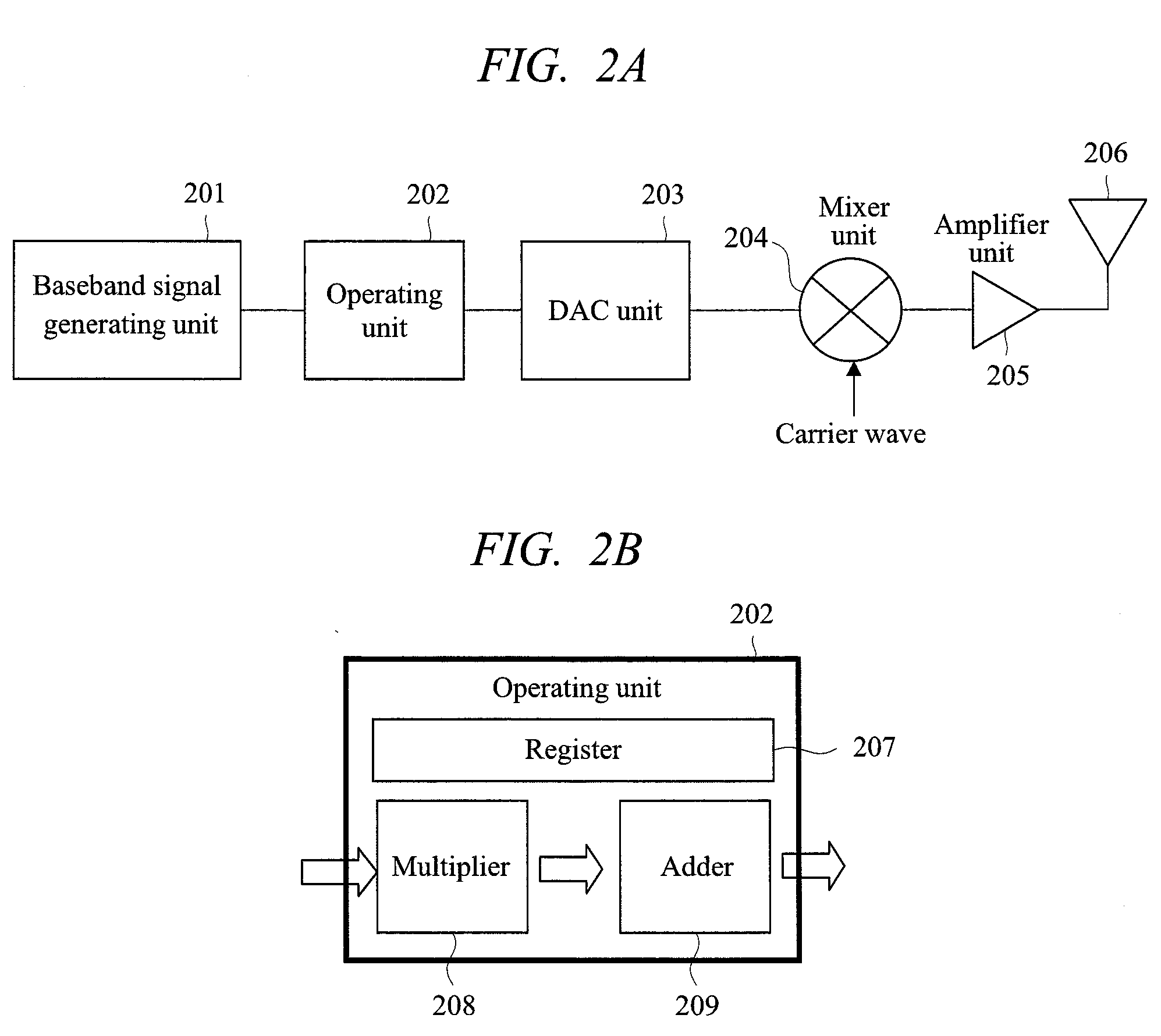
[0079]FIG. 2A is a block diagram showing a configuration of a semiconductor integrated circuit device according to an embodiment 1 of the present invention, and FIG. 2B is a block diagram showing a configuration of an operating unit 202 shown in FIG. 2A.
[0080]First, referring to FIGS. 2A and 2B, an example of the configuration of the semiconductor integrated circuit device according to the embodiment 1 is described. The semiconductor integrated circuit device according to the embodiment 1 is, for example, a semiconductor integrated circuit device (IC) used in a radio transmitter such as a reader-writer in the UHF band electronic tag (RFID) system, and is formed on one semiconductor chip using a known semiconductor manufacturing technique. The semiconductor integrated circuit device having the radio transmission function consists of, for example, a baseband signal generating unit 201, which generates data for transmission, an operating unit202, which consists of a multiplier 208, an ...
embodiment 2
[0095]FIGS. 4A and 4B are block diagrams showing configuration of a semiconductor integrated circuit device according to an embodiment 2.
[0096]The semiconductor integrated circuit device according to the embodiment 2 is an example in which a digital filter 401 is inserted between the baseband signal generating unit 201 and the DAC unit 203 of the semiconductor integrated circuit device of the embodiment 1.
[0097]The operating unit 202 and the digital filter 401 are both logical operations, and therefore either of them can be carried out first. And therefore, the digital filter 401 can be put behind the operating unit 202 as shown in FIG. 4A, or before the operating unit 202.
[0098]By adding the digital filter, the waveform at risings and failings is more smoothed.
embodiment 3
[0099]FIG. 5 is a block diagram showing a configuration of a semiconductor integrated circuit device according to an embodiment 3 of the present invention.
[0100]The semiconductor integrated circuit device according to the embodiment 3 is an example in which a circulator 501 which separates a transmission signal and a reception signal, a receiver unit 502 which receives a modulated wave, a demodulating unit 503 which extracts original data from the modulated wave, and a reception condition determining unit 504 which determines a reception condition of addition are added to the semiconductor integrated circuit device (FIG. 4A) of the embodiment 2.
[0101]The reception condition determining unit 504 performs the determination on the basis of the original data demodulated by the demodulation unit 503, and the operation coefficients in the register 207 are changed on the basis of a result of the determination.
[0102]In a communication system that performs backscatter communication, a transm...
PUM
 Abstract
Description
Claims
Application Information