Selective growth method, nitride semiconductor light emitting device and manufacturing method of the same

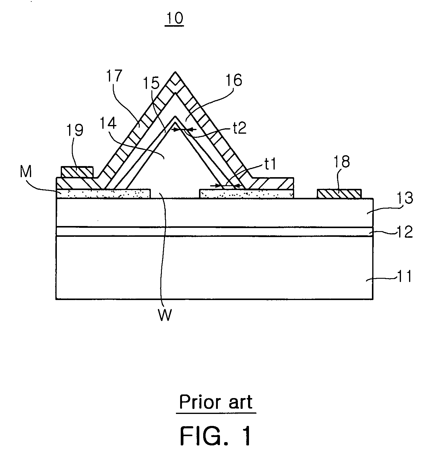
a semiconductor and light emitting device technology, applied in the direction of polycrystalline material growth, crystal growth process, chemically reactive gas, etc., can solve the problem of hardly obtaining the light of a desired wavelength, nitride crystals are accompanied by many crystal defects, and the nitride light structure of the hexagonal pyramid experiences a difference in the growth rate between the base and the apex,

Active Publication Date: 2008-02-14
SAMSUNG ELECTRONICS CO LTD
View PDF8 Cites 5 Cited by
  • Summary
  • Abstract
  • Description
  • Claims
  • Application Information

AI Technical Summary

Benefits of technology

[0037]wherein the first conductive nitride semiconductor crystal has at least one intermediate stress-relieving area having crystal planes inclined at a greater angle than those of upp...

Problems solved by technology

A nitride crystal is accompanied by many crystal defects due to absence of an adequate substrate for growth thereof.
However, despite the aforesaid advantages, the conventional nitride light structure of the hexagonal pyramid experiences a difference in the growth rate between the base and the apex of the pyramidal structure due to stress caused by the inclined side surfaces.
That is...

Method used


Image

  • Selective growth method, nitride semiconductor light emitting device and manufacturing method of the same
  • Selective growth method, nitride semiconductor light emitting device and manufacturing method of the same
  • Selective growth method, nitride semiconductor light emitting device and manufacturing method of the same

Examples


example

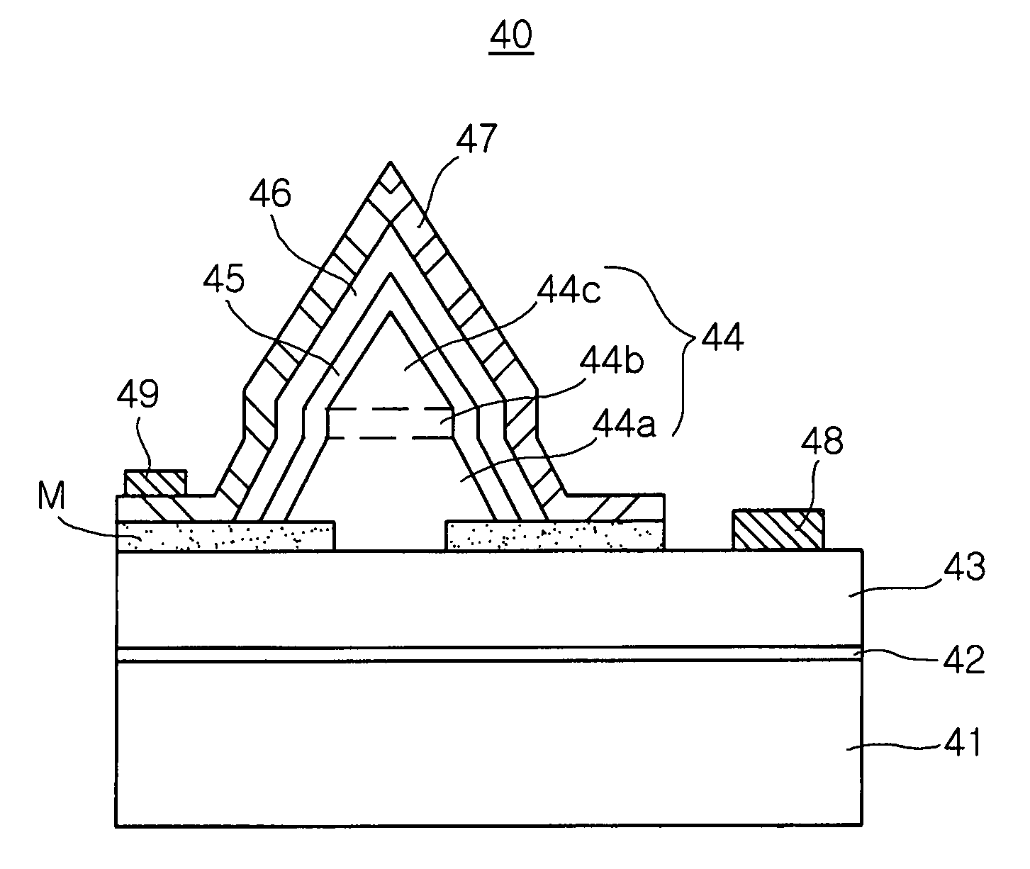
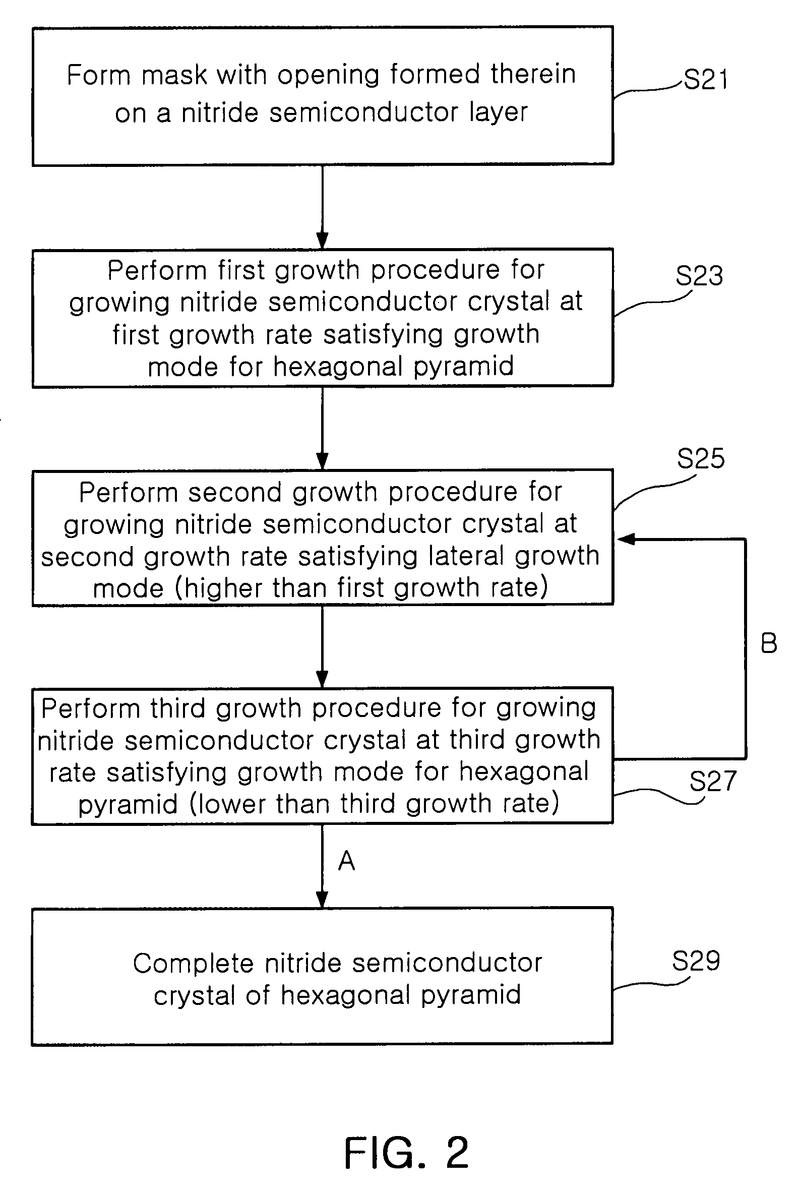
[0072]A low-temperature buffer layer was formed on a sapphire substrate and an n-type GaN layer was formed as a base layer via Metal Organic Chemical Vapor Deposition (MOCVD). Then, a SiO2 mask having an opening with a diameter of about 4 μm was formed on the n-type GaN layer.

[0073]To grow a hexagonal pyramid, a GaN crystal was grown at a temperature of 950° C. and at a growth rate of about 8 μm / hr for an hour. Here, a growth pressure was 400 torr and a group V / III ratio was about 3,000. Then, to allow the GaN crystal to grow more laterally, a flow rate of trimethyl gallium (TMG) was increased to raise a growth rate to about 10 μm / hr with other conditions maintained constant, repeating a growth process for the intermediate stress-relieving area. The growth process for the intermediate stress-relieving area continued for about five minutes and then the n-type GaN crystal of a hexagonal pyramid was grown under the same condition as previously adopted.

[0074]FIGS. 5a and 5b illustrate t...


PUM


Abstract

A method for selectively growing a nitride semiconductor, in which a mask is formed, with an opening formed therein, on a nitride semiconductor layer. A nitride semiconductor crystal is selectively grown on a portion of the nitride semiconductor layer exposed through the opening in the mask, the nitride semiconductor crystal shaped as a hexagonal pyramid and having crystal planes inclined with respect to a top surface of the nitride semiconductor. Here, the nitride semiconductor crystal has at least one intermediate stress-relieving area having crystal planes inclined at a greater angle than those of upper and lower areas of the nitride semiconductor crystal, the intermediate stress-relieving area relieving stress which occurs from continuity in the inclined crystal planes.

Description

CLAIM OF PRIORITY[0001]This application claims the benefit of Korean Patent Application No. 2006-75407 filed on Aug. 9, 2006 in the Korean Intellectual Property Office, the disclosure of which is incorporated herein by reference.BACKGROUND OF THE INVENTION[0002]1. Field of the Invention[0003]The present invention relates to a method for growing a nitride semiconductor, and more particularly, to a method for selectively growing a nitride semiconductor of a hexagonal pyramid, a nitride light emitting device manufactured using the same method and a manufacturing method of the same device.[0004]2. Description of the Related Art[0005]Recently, a semiconductor light emitting device has been vigorously studied as a new light source to replace a filament-based bulb and a fluorescent lamp. Especially, attention has been drawn on a study on a light emitting diode (LED) using a nitride compound semiconductor such as GaN. A nitride crystal is accompanied by many crystal defects due to absence o...

Claims


Application Information

Patent Timeline
IPC IPC(8): H01L29/24H01L21/36H01L33/00H01L33/06H01L33/16H01L33/24H01L33/32
CPCC30B25/02C30B25/04C30B29/406H01L21/0237H01L33/24H01L21/0254H01L21/02639H01L21/02647H01L33/007H01L21/02458
Inventor PARK, HEE SEOKPARK, GIL HANYOO, SANG DUKPARK, YOUNG MINKIM, HAK HWANMYOUNG, SEON YOUNGLEE, SANG BUMPARK, KI TAEJUNG, MYOUNG SIKMIN, KYEONG IK
Owner SAMSUNG ELECTRONICS CO LTD
Why Eureka
Try Eureka