Inverted-trench grounded-source fet structure using conductive substrates, with highly doped substrates

a ground source and fet technology, applied in the field of inverted-trench grounded source field effect transistor (fet) structure, can solve the problem of low manufacturing cost, and achieve the effect of reducing cell pitch, low manufacturing cost and low manufacturing cos

Active Publication Date: 2008-02-14
ALPHA & OMEGA SEMICON LTD
View PDF2 Cites 100 Cited by
  • Summary
  • Abstract
  • Description
  • Claims
  • Application Information

AI Technical Summary

Benefits of technology

[0009]It is therefore an aspect of the present invention to provide a new and improved inverted ground-source trenched FET on highly doped substrate, e.g., highly doped P+ substrate, with a bottom-source and top-drain having a reduced cell pitch thus achieving low manufacturing cost. The low manufacturing cost is achieved because a low effective die cost with a reduce cell pitch when the improved device configuration is implemented. The above discussed technical difficulties and limitations of not able to shrink the cell pitch as encountered in the conventional semiconductor power devices are therefore overcome.
[0010]Specifically, it is an aspect of the present invention to provide a new and improved inverted ground-source trenched FET on highly doped substrate, e.g., highly doped P+ substrate, with a bottom-source and top-drain that has a significant reduce source inductance by eliminating the source wires and meanwhile minimizing the specific on resistance Rsp by using an integrated body-source short structure at the lower portion of the trenches surrounded by the gate electrodes.
[0011]It is another aspect of the present invention to provide a new and improved inverted ground-source trenched FET on highly doped substrate, e.g., highly doped P+ substrate, with a bottom-source and top-drain that are scalable for compatible with applications over a range of high and low voltages. The semiconductor power devices as disclosed in this invention further achieve rugged and reliable performance with reduced possibility of latch up, reduced hot carrier injection and peak voltage generation away from gate oxide, etc. because of the distributed body contact configurations.
[0012]It is another aspect of the present invention to provide a new and improved inverted ground-source trenched FET on highly doped substrate, e.g., highly doped P+ substrate, with a bottom-source and top-drain that are scalable for providing a vertical current channel with controllable drift region length such that it is more adaptable for pitch reduction configurations. The bottom source connection is established through a conductive substrate and a source contact formed at the bottom of the trench in direct contact with the highly doped substrate. The requirement for using a deep resistive sinker or a trench contact is therefore eliminated.
[0013]It is another aspect of the present invention to provide a new and improved inverted ground-source trenched FET on highly doped substrate, e.g., highly doped P+ substrate, with a bottom-source and top-drain with reduced gate-drain capacitance by forming a thicker oxide layer over the drain extension to reduce the drain-to-gate capacitance Cgd to increase the break down voltage (BV).
[0014]It is another aspect of the present invention to provide a new and improved inverted ground-source trenched FET on highly doped substrate, e.g., highly doped P+ substrate, with a bottom-source and top-drain with the termination region formed outside the continuous gate ring structure. In a preferred embodiment, a typical layout of this structure is based on a closed cell configuration. The N-drift region in this configuration is left unconnected because there is no contact to the termination region. Since the substrate is at the source potential that is ground potential for an NMOS device, the floating N-drift region is likely operates at a ground potential to provide a self-termination. The device configuration further has an advantage that any damage from the sawing of the dies in the scribing region will tend to short the floating N-drift regions to the grounded substrate.

Problems solved by technology

The low manufacturing cost is achieved because a low effective die cost with a reduce cell pitch when the improved device configuration is implemented.

Method used


Image

  • Inverted-trench grounded-source fet structure using conductive substrates, with highly doped substrates
  • Inverted-trench grounded-source fet structure using conductive substrates, with highly doped substrates
  • Inverted-trench grounded-source fet structure using conductive substrates, with highly doped substrates

Examples


Embodiment Construction

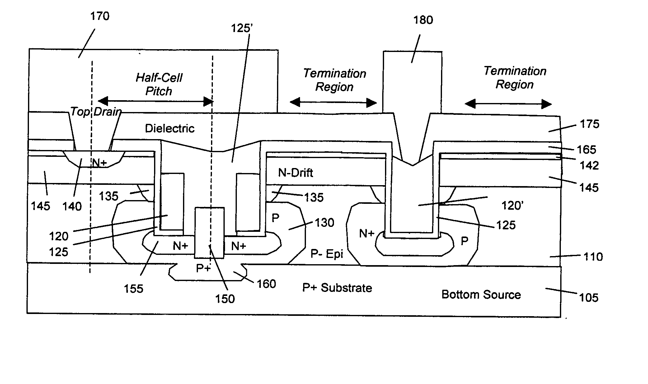
[0025]Referring to FIG. 2 for a cross sectional view of an N-channel inverted ground-source trenched FET device with a bottom source and a top drain of this invention. The inverted ground-source trenched N-channel FET device is supported on a P+ substrate 105 functioning as a bottom source electrode. Alternatively a P-channel device may be formed over a N+Si substrate or other substrate such as silicon carbide, GaN, or other kinds of semiconductor substrates, etc. A layer of P-epitaxial layer 110 is supported on top of the substrate 105. The substrate is configured with an active cell area and a termination area typically disposed on the peripheral of the substrate. The FET device 100 has a plurality of trenches opened from the top surface of the substrate to reach to a lower portion of the epitaxial layer 110. The trenches opened in the active cell area is wider to form a gate with gate polysilicon layer attached to the sidewalls of the trench with the sidewalls of the trenches pad...


PUM


Abstract

This invention discloses an improved trenched metal oxide semiconductor field effect transistor (MOSFET) device that includes a trenched gate surrounded by a source region encompassed in a body region above a drain region disposed on a bottom surface of a substrate. The MOSFET cell further includes a shielded gate trench (SGT) structure below and insulated from the trenched gate. The SGT structure is formed substantially as a round hole having a lateral expansion extended beyond the trench gate and covered by a dielectric linen layer filled with a trenched gate material. The round hole is formed by an isotropic etch at the bottom of the trenched gate and is insulated from the trenched gate by an oxide insulation layer. The round hole has a lateral expansion beyond the trench walls and the lateral expansion serves as a vertical alignment landmark for controlling the depth of the trenched gate. The MOSFET device has a reduced gate to drain capacitance Cgd depending on the controllable depth of the trenched gate disposed above the SGT structure formed as a round hole below the trenched gate.

Description

BACKGROUND OF THE INVENTION[0001]1. Field of the Invention[0002]The invention relates generally to the semiconductor power devices. More particularly, this invention relates to an inverted-trench grounded source field effect transistor (FET) structure that uses a conductive substrate with highly doped P+ substrate.[0003]2. Description of the Prior Art[0004]Conventional technologies to further reduce the source inductance for semiconductor power devices including the source inductance in FET, MOSFET and JFET devices are challenged by several technical difficulties and limitations. Specifically, there are technical challenges faced by those of ordinary skill in the art to reduce the source inductance. Meanwhile, there are ever increasing demand to reduce the source inductance in the semiconductor power devices because more and more power devices are required for applications that demand these devices to function with high efficiency, high gain, and high frequency. Generally, reduction...

Claims


Application Information

Patent Timeline
Patent Type & Authority Applications(United States)
IPC IPC(8): H01L29/94
CPCH01L21/26586H01L29/0865H01L29/0878H01L29/0886H01L29/407H01L29/4175H01L29/7825H01L29/66689H01L29/66704H01L29/66719H01L29/66734H01L29/781H01L29/7811H01L29/4236
Inventor HEBERT, FRANCOIS
Owner ALPHA & OMEGA SEMICON LTD
Why Eureka
Try Eureka