Organic El Element, Organic El Display Apparatus, Method for Manufacturing organic El Element, and Apparatus for Manufacturing Organic El Element

a technology of organic el and display apparatus, which is applied in the direction of discharge tube luminescnet screen, non-electron-emitting shielding screen, natural mineral layered product, etc., can solve the problems of organic el layer short circuit, drive voltage increase, and ultimately short circuit and destruction of organic el layer, so as to improve the reproducibility of the thickness of the obtained film and improve the concentration of components.

Active Publication Date: 2008-02-14
UDC IRELAND
View PDF8 Cites 24 Cited by
  • Summary
  • Abstract
  • Description
  • Claims
  • Application Information

AI Technical Summary

Benefits of technology

[0023]According to the apparatus for manufacturing an organic EL element, the deposition source is moved in the direction from the first side toward the second side or in the direction from the second side toward the first side when an organic layer of the organic EL element is formed, whereby effects of improving the reproducibility of the thickness of the obtained film and of improving the reproducibility of the concentrations of components added to the film can be obtained.

Problems solved by technology

It is known that the optical output is decreased and the drive voltage is increased over time when the organic EL element is used for a long time, and the organic EL layer is ultimately short-circuited and destroyed when the operation thereof is further continued.
Further, it is assumed that deterioration of the electrodes due to oxidation is also a cause for the destruction.
In the foregoing case where the acceptor is doped in the hole transport layer, the conductivity is improved; however, there is a problem in that a current flow is generated upon application of voltage in the negative direction owing to insufficient confinement of the carriers, in other words, a leak current is generated.
However, the leak current cannot be sufficiently suppressed in any of the foregoing organic EL elements.
In this case, when the leak current generated by a voltage in a negative direction is large in an element b, crosstalk is generated in the element b. In the case where the leak current is large owing to insufficient confinement of the electrons, there is a problem in that the luminous efficiency is decreased because the proportion of the electrons contributing to light emission is reduced.
Thus, it was difficult to suppress the leak current while improving the conductivity of the organic EL element and suppressing the operation voltage thereof in the conventional organic EL element.

Method used


Image

  • Organic El Element, Organic El Display Apparatus, Method for Manufacturing organic El Element, and Apparatus for Manufacturing Organic El Element
  • Organic El Element, Organic El Display Apparatus, Method for Manufacturing organic El Element, and Apparatus for Manufacturing Organic El Element
  • Organic El Element, Organic El Display Apparatus, Method for Manufacturing organic El Element, and Apparatus for Manufacturing Organic El Element

Examples


example 1

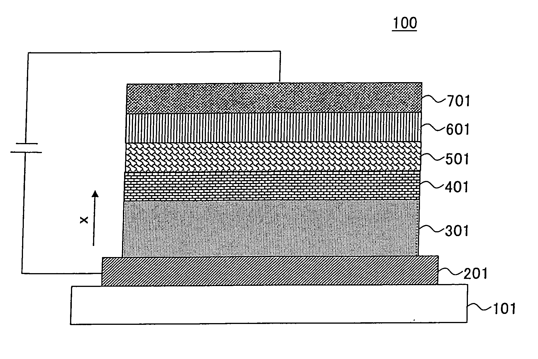
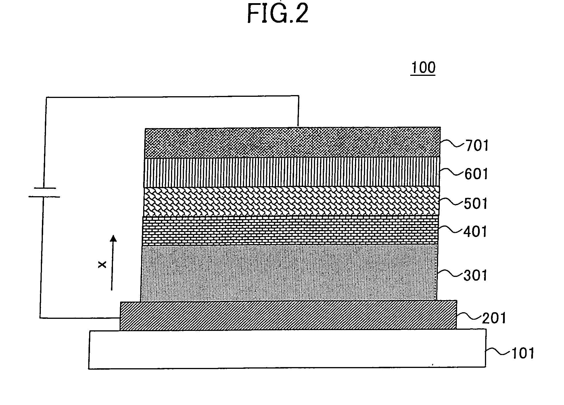
[0063]FIG. 4A shows an example in which the hole injection layer 301A shown in FIG. 3A is used as the hole injection layer in the organic EL element shown in FIG. 2. The accompanying graph schematically shows the concentration of the acceptor in the hole injection layer. In the drawing, the parts described above are represented by the same reference characters and the descriptions thereof are omitted. In the drawing, components other than the hole injection layer, the positive electrode and the hole transport layer are omitted, and the x-axis direction shown in this figure corresponds to the x-axis direction shown in FIG. 2 (the same holds true for FIGS. 4B to 4C).

[0064]In the example, a substrate formed from glass was used as the substrate 101, an ITO electrode was used as the positive electrode 201, 2-TNATA (4,4′,4″-tris(2-naphthylphenyl amino)triphenylamine, manufactured by BANDO CHEMICAL INDUSTRIES, LTD) was used as the hole injection layer 301A, F4-TCNQ (2,3,5,6-tetrafluoro-7,7...

example 2

[0075]FIG. 4B shows the example in which the hole injection layer 301B shown in FIG. 3B is used as the hole injection layer in the organic EL element shown in FIG. 2. The accompanying graph schematically shows the concentration of the acceptor in the hole injection layer.

[0076]In this example, the structures of the substrate 101, the positive electrode 201, the hole transport layer (electron suppression layer) 401, the luminescent layer 501, the electron transport layer 601 and the negative electrode 701 are the same as in Example 1, and can be produced by the method described in Example 1.

[0077]In this example, similarly to Example 1, 2-TNATA was used as the hole injection layer 301B, and F4-TCNQ was used as the acceptor doped in the hole injection layer when the hole injection layer 301B is formed on the ITO surface as follows.

[0078]First, 2-TNANA and F4-TCNQ were deposited to a thickness of 30 nm (0.12%) at the deposition speed of 0.1 nm / s and 0.00012 nm / s, respectively, so that ...

example 3

[0082]FIG. 4C shows an example in which the hole injection layer 301C shown in FIG. 3C is used as the hole injection layer in the organic EL element shown in FIG. 2. The accompanying graph schematically shows the acceptor concentration of the hole injection layer.

[0083]In this example, the structures of the substrate 101, the positive electrode 201, the hole transport layer (electron suppression layer) 401, the luminescent layer 501, the electron transport layer 601 made of Alq, and the negative electrode 701 are the same as in Example 1, and can be formed by the method described in Example 1.

[0084]In this example, similarly to Example 1, 2-TNATA was used as the hole injection layer 301C, and F4-TCNQ was used as the acceptor doped in the hole injection layer when the hole injection layer 301C was formed on the surface of the ITO as follows.

[0085]First, 2-TNANA and F4-TCNQ were deposited to a thickness of 10 nm (0.04%) at the deposition speeds of 0.1 nm / s and 0.00004 nm / s, respective...


PUM

PropertyMeasurementUnit
thicknessaaaaaaaaaa
pressureaaaaaaaaaa
thicknessaaaaaaaaaa

Abstract

An object of the present invention is to enable suppression of a leak current of an organic EL element while improving a conductivity of the organic EL element and suppressing an operation voltage thereof. An organic EL element is used which comprises at least a luminescent layer, a hole transport layer adjacent to a positive-electrode side of the luminescent layer, and an electron injection transport layer adjacent to a negative-electrode side of the luminescent layer, wherein a hole injection layer is provided between the hole transport layer and the positive electrode, and the conductivity of the hole injection layer continuously changes along a thickness direction of the hole injection layer.

Description

TECHNICAL FIELD [0001]The present invention relates to an organic EL element, an organic EL element display apparatus, a method for manufacturing an organic element, and an apparatus for manufacturing an organic EL element.RELATED ART[0002]In recent years, a flat display apparatus whose thickness can be reduced has been increasingly put into practical use in place of conventionally used CRT (Cathode Ray Tube). An organic electroluminescence element, which is characterized in its self-luminous property and high-speed response (hereinafter, referred to as organic EL element in this specification), has been attracting attention as a next-generation display apparatus.[0003]The organic EL element has a structure where an organic EL layer, which is a luminescent layer, is sandwiched between a positive electrode and a negative electrode. In the structure, holes are injected into the organic EL layer from the positive electrode and electrons are injected thereinto from the negative electrod...

Claims


Application Information

Patent Timeline
Patent Type & Authority Applications(United States)
IPC IPC(8): B32B9/00B05D5/12H01J19/40H01L51/00H01L51/50H05B33/14H05B33/22
CPCH01L51/0054H01L51/006H01L51/0071H01L2251/5346H01L51/0081H01L51/5088H01L51/0072H10K85/622H10K85/633H10K85/6572H10K85/657H10K85/324H10K50/17H10K2101/80
Inventor ITAI, YUICHIROSATOH, TASUKUSAKAMOTO, YOSHIAKITAKAHASHI, TOSHIROKINOSHITA, MASARU
Owner UDC IRELAND
Why Eureka
Try Eureka