Materials and methods of forming controlled void
a technology of controlled voids and materials, applied in the direction of basic electric elements, electrical apparatus, semiconductor devices, etc., can solve the problems of capillary effect and collapse of small structures, and the process may not be amenable to the current dual damascene process used in copper integration
- Summary
- Abstract
- Description
- Claims
- Application Information
AI Technical Summary
Problems solved by technology
Method used
Image
Examples
first embodiment
Organic Labile Sacrificial Materials
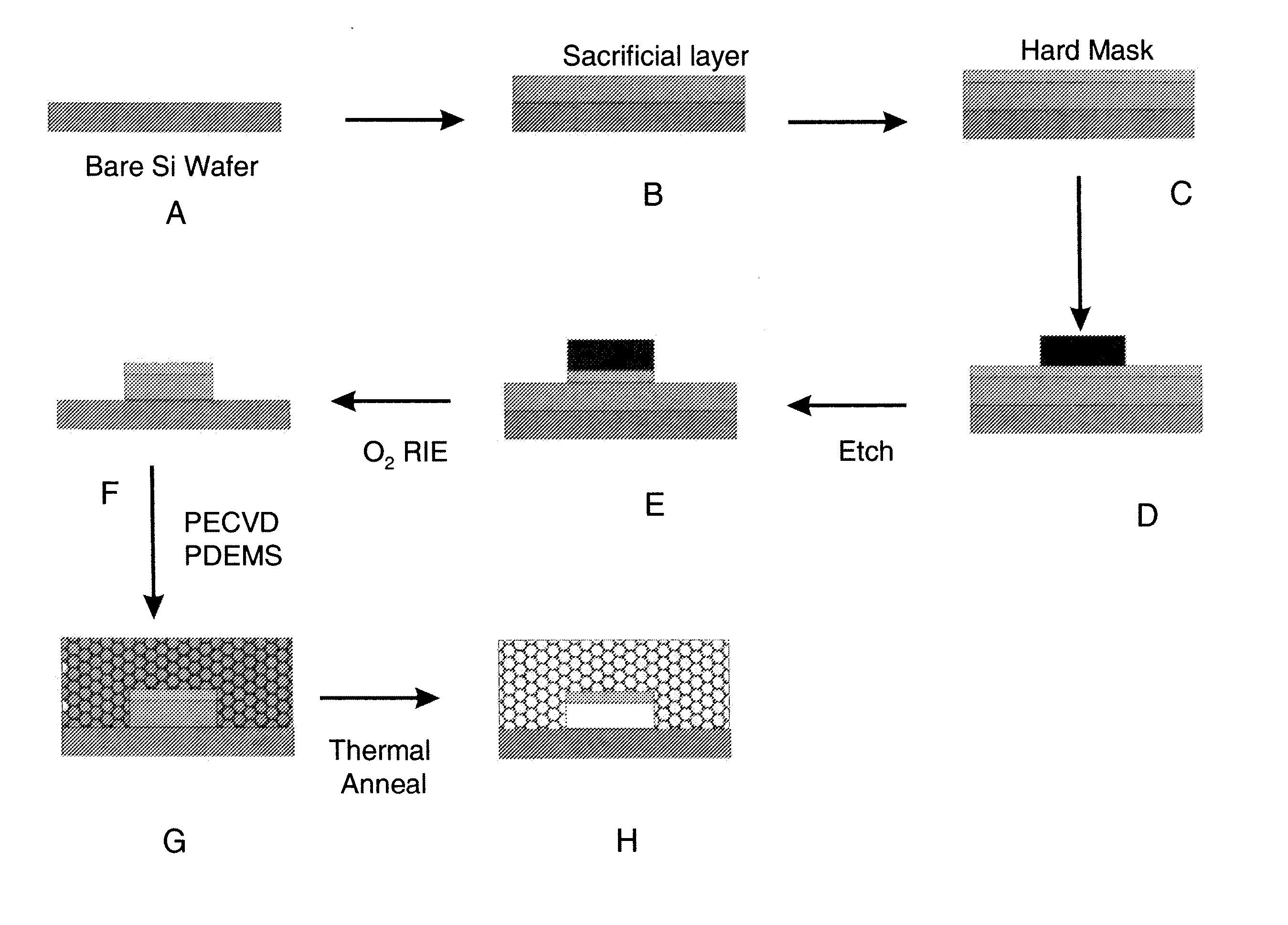
[0052] In this embodiment a sacrificial organic layer is used to create the void space. By using the at least one same organic precursor for deposition of both the sacrificial layer and for use as a porogen in the composite layer, for example a PDEMS™ layer it allows for a gradient to be built into the device. Because the same precursor is used as the organic precursor for the sacrificial layer and the as the organic porogen precursor the PECVD process can be run initially using just the at least one organic precursor followed by flowing an additional at least one OSG precursor a seamless gradient can be formed between the sacrificial layer and the porous layer. U.S. Pat. Nos. 6,583,048 and 6,846,515, 6,054,206, 6,054,379, 6,171,945, and WO 99 / 41423 provide some exemplary CVD methods that may be used to form the organosilicate film of the present invention.
[0053] Without being bound by theory the nature of the organic precursor used to deposit b...
second embodiment
Sacrificial Materials of Selectively Etched Silicon
[0090] It is known that a fluorine containing selective etching gas (for example XeF2 or BrF3) in the gas phase, will selectively etch silicon versus silicon dioxide, for example see Lopez et. al. in Micro Total Analysis Systems 2002, Proceedings of the μTAS 2002 Symposium, 6th, Nara, Japan, Nov. 3-7, 2002 (2002), 2 934-936 The etch selectivity results from the increased chemical reactivity of single crystal- poly- or amorphous-silicon with the XeF2, BrF3 etc being used. One example of this type of fabrication would be to form a cantilever by depositing a layer of poly-silicon into SiO2 on Silicon and then coating with a second layer of SiO2 on top of the poly-silicon, after patterning and etching both the top SiO2 layer and the poly-silicon layer the cantilever can be released by selectively etching the poly-silicon layer using XeF2. In this example the poly-silicon is etched from the edges inward as the XeF2 diffuses under the Si...
third embodiment
Sacrificial Materials Solvated in Polar Solvents
[0100] The use of a porous silicate layer and a water soluble metal oxide, such as germanium oxide (GeO2), to fabricate structures is also contemplated as an embodiment of the present invention. It is known that GeO2 is a water soluble oxide material, and that GeO2 can be deposited by any of a number of techniques such as chemical vapor deposition or PECVD from readily available precursor materials or from spin-on techniques usign pre-oxides followed by an anneal step. Examples of precursors for the formation of a water soluble metal oxide are materials such as, but not limited to, germanium (Ge) based precursor is selected from the group consisting of tetra-methyl germane, germane, tetra-methoxy germanium and tetra-ethoxy germanium; and the boron (B) based precursor is selected from the group consisting of tri-methyl boron, trimethoxy borane, triethoxy borane and diborane. At the same time SiO2 and OSG films are not water soluble, bu...
PUM
| Property | Measurement | Unit |
|---|---|---|
| exposure time | aaaaa | aaaaa |
| power | aaaaa | aaaaa |
| dielectric constant | aaaaa | aaaaa |
Abstract
Description
Claims
Application Information


