Method of selectively removing conductive material

a technology of conductive metal and substrate, applied in electrodialysis, refrigeration machines, refrigeration components, etc., can solve the problems of difficult removal of most barrier materials by cmp, brittle current low-k and future ultra-low-k dielectrics, dishing and scratching, etc. selective removal of conductive metals is facilitated, the effect of facilitating the removal of conductive metals

Inactive Publication Date: 2008-02-21
MICRON TECH INC
View PDF30 Cites 28 Cited by
  • Summary
  • Abstract
  • Description
  • Claims
  • Application Information

AI Technical Summary

Benefits of technology

[0008]The present compositions and methods facilitate removal of conductive metal(s) selectively relative to dielectric material in an electrolyte process without surface contact by a processing pad or the application of an external...

Problems solved by technology

Current low-k and future ultra low-k dielectrics are brittle and sensitive to the mechanical stresses needed to physically remove refractory metals, such as tantalum (Ta).
Most barrier materials are difficult to remove by CMP because the barrier materials resist removal by abrasion and dissolution.
Typical barrier removal slurries require a high abrasive concentration, which tend to result in dishing and scratching of the copper interconnect 20 within the openings 14 and detrimental erosion to the exposed insulating layer 12, including peeling and delaminating of low k dielect...

Method used


Image

  • Method of selectively removing conductive material
  • Method of selectively removing conductive material
  • Method of selectively removing conductive material

Examples


Embodiment Construction

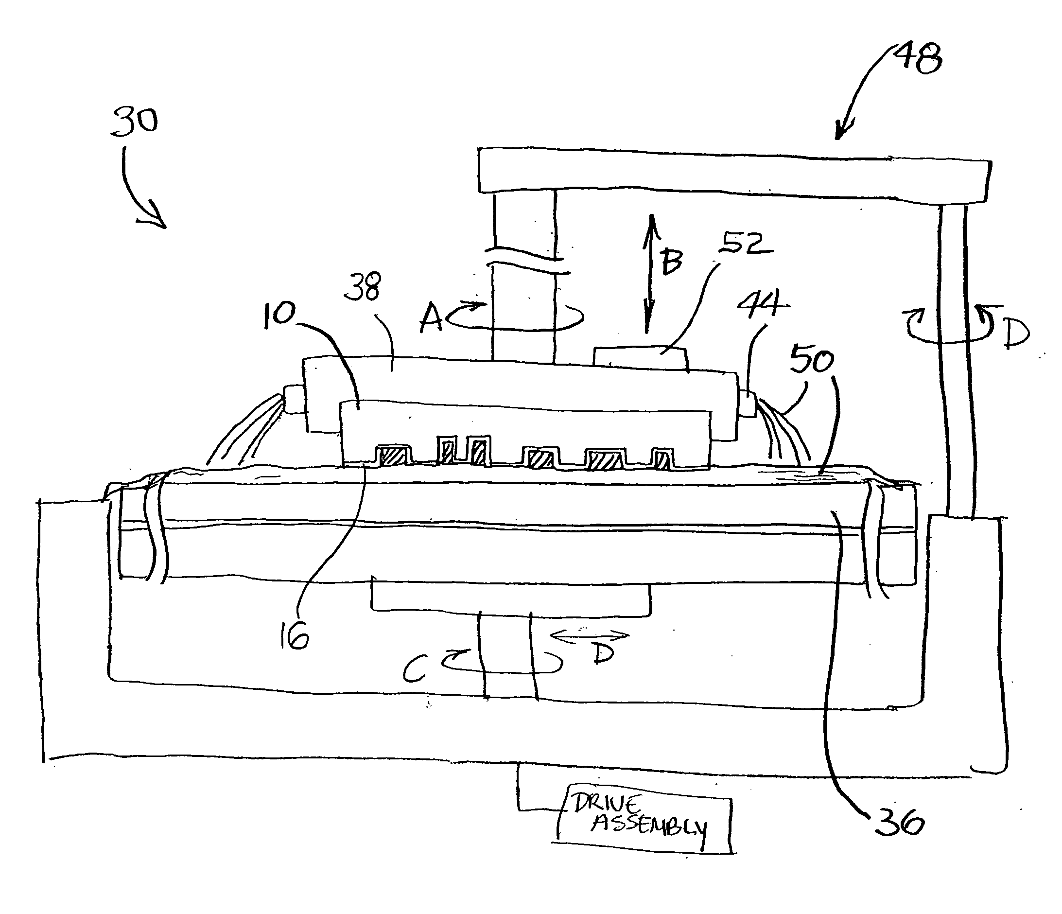
[0032]The following description with reference to the drawings provides illustrative examples of devices, assemblies, systems, and methods for selectively removing conductive metal material from semiconductor wafers and other substrates according to the invention. Such description is for illustrative purposes only and not for purposes of limiting the same. The present invention can be utilized to provide other embodiments of devices, assemblies, and systems in accordance with the invention.

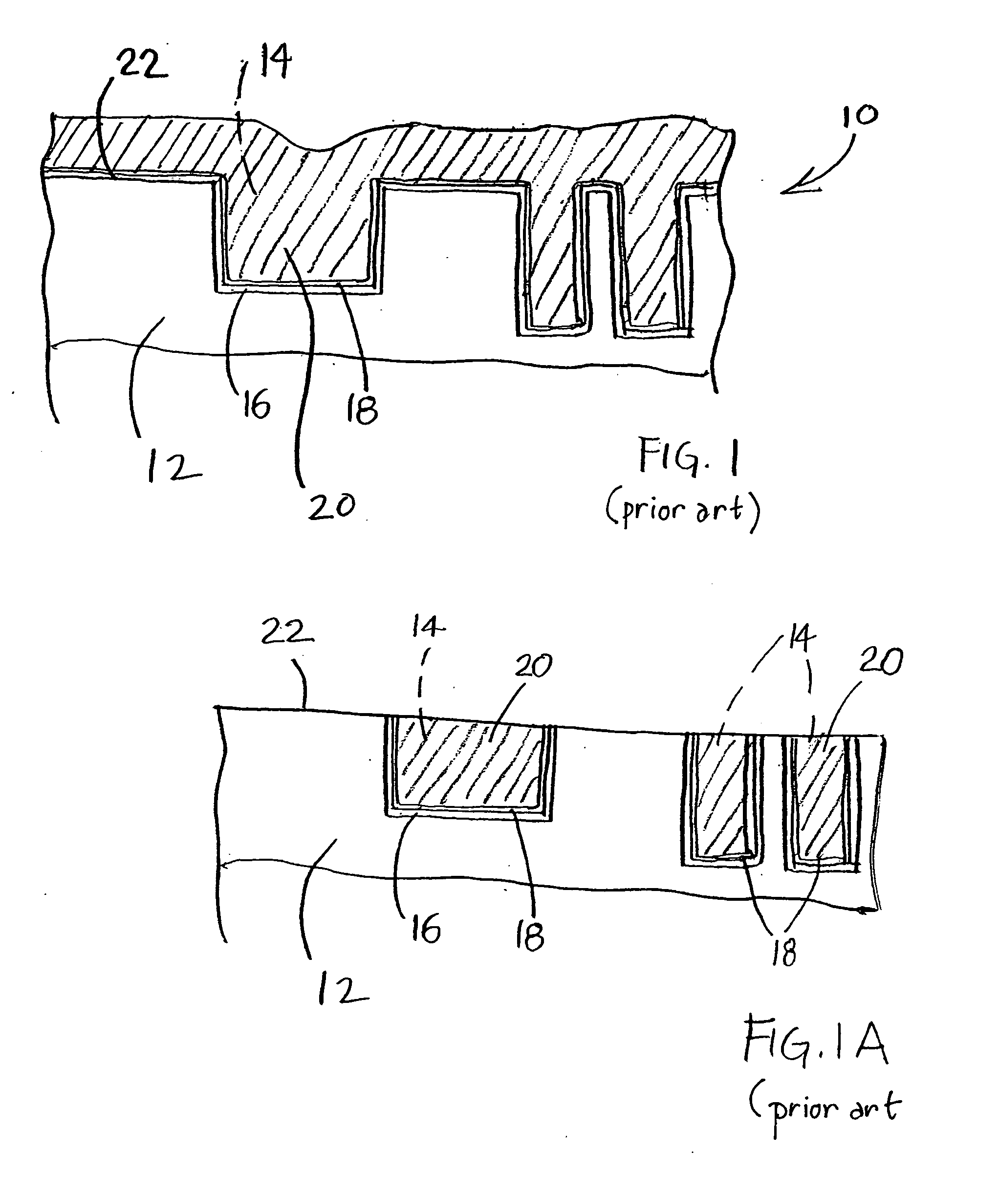
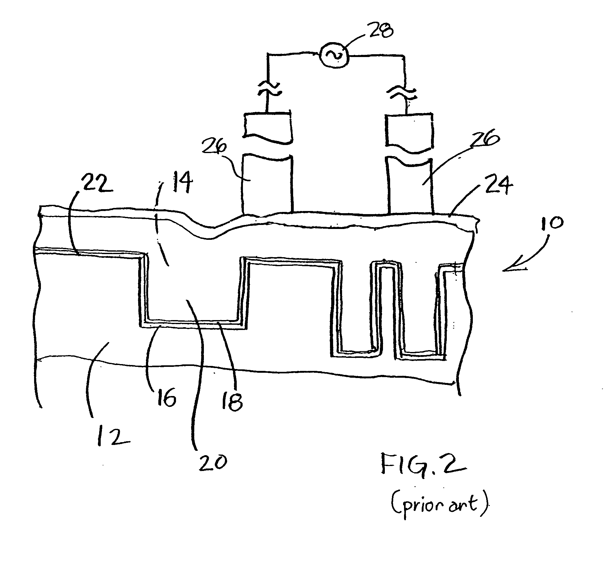
[0033]In the context of the current application, the term “semiconductor substrate” or “semiconductive substrate” or “semiconductive wafer fragment” or “wafer fragment” or “wafer” will be understood to mean any construction comprising semiconductor material, including but not limited to bulk semiconductive materials such as a semiconductor wafer (either alone or in assemblies comprising other materials thereon), and semiconductive material layers (either alone or in assemblies comprising other mat...


PUM

PropertyMeasurementUnit
Pressureaaaaaaaaaa
Weightaaaaaaaaaa
Pressureaaaaaaaaaa

Abstract

An electrolyte solution, methods, and systems for selectively removing a conductive metal from a substrate are provided. The electrolyte solution comprising nanoparticles that are more noble than the conductive metal being removed, is applied to a substrate to remove the conductive metal selectively relative to a dielectric material without application of an external potential or contact of a processing pad with the surface of the substrate. The solutions and methods can be applied, for example, to remove a conductive metal layer (e.g., barrier metal) selectively relative to dielectric material and to a materially different conductive metal (e.g., copper interconnect) without application of an external potential or contact of a processing pad with the surface of the substrate.

Description

FIELD OF THE INVENTION[0001]The invention relates generally to semiconductor processing for forming contacts and other features, and more particularly to methods and systems for selectively removing conductive metal(s) from a substrate.BACKGROUND OF THE INVENTION[0002]In the fabrication of semiconductor devices, contact holes and other features that are formed on a substrate are filled with a conductive material to provide contacts and other circuitry. One method for forming vertical and horizontal interconnects is by a damascene or dual damascene method. FIG. 1 illustrates a portion of a substrate 10 (e.g., wafer or microelectronic substrate) having conductive elements formed according to a prior art damascene method. The substrate 10 includes an insulating layer 12 (e.g., an interdielectric layer or ILD) deposited onto the substrate 10 and pattern etched to form interconnect openings 14. A barrier material layer 16, for example, tantalum (Ta), is deposited within the openings 14 t...

Claims


Application Information

Patent Timeline
IPC IPC(8): B01D35/06
CPCB82Y30/00C23F1/02C23F1/10H01L21/67086H01L21/32115H01L21/67075H01B1/122
Inventor KLEIN, RITA J.COLLINS, DALE W.MORGAN, PAULGREELEY, JOSEPH N.SINHA, NISHANT
Owner MICRON TECH INC
Why Eureka
Try Eureka