Multi-layered chalcogenide and related devices having enhanced operational characteristics

a technology of chalcogenide and operational characteristics, applied in the field of chalcogenide materials, can solve the problems of undesirable variability in either the set resistance or reset resistance of chalcogenide memory devices, and achieve the effects of less stringent conditioning requirements for device operation, reduced interface resistance, and reduced reset curren

Inactive Publication Date: 2008-02-21
OVONYX
View PDF4 Cites 41 Cited by
  • Summary
  • Abstract
  • Description
  • Claims
  • Application Information

AI Technical Summary

Benefits of technology

[0018] The instant invention provides exemplary embodiments of chalcogenide memory and switching devices that include an active region that includes a memory or switching material extending between two electrical terminals. In one embodiment, the active region includes two or more layers and at least one of the layers includes a chalcogenide material. In another embodiment, at least one of the layers of the active region is a heterogeneous layer that includes a chalcogenide material and a promoter material distributed as a component within. The promoter component is distributed as one or more discrete regions within the heterogeneous layer and provides performance benefits such as reduced interface resistance between the heterogeneous layer and an electrical contact, less stringent conditioning requirements for device operation, lower reset current, greater contrast between the reset resistance and set resistance of the active region, and enhanced set speed of the active region.

Problems solved by technology

An outstanding problem that has been identified in the prior art concerns the variability of the set and / or reset resistance of chalcogenide memory devices in the first several cycles of operation of the as-fabricated device.
For practical memory applications, variability in either the set resistance or reset resistance is undesirable because those resistances are commonly used as indicators for the memory states.

Method used


Image

  • Multi-layered chalcogenide and related devices having enhanced operational characteristics
  • Multi-layered chalcogenide and related devices having enhanced operational characteristics
  • Multi-layered chalcogenide and related devices having enhanced operational characteristics

Examples


example 1

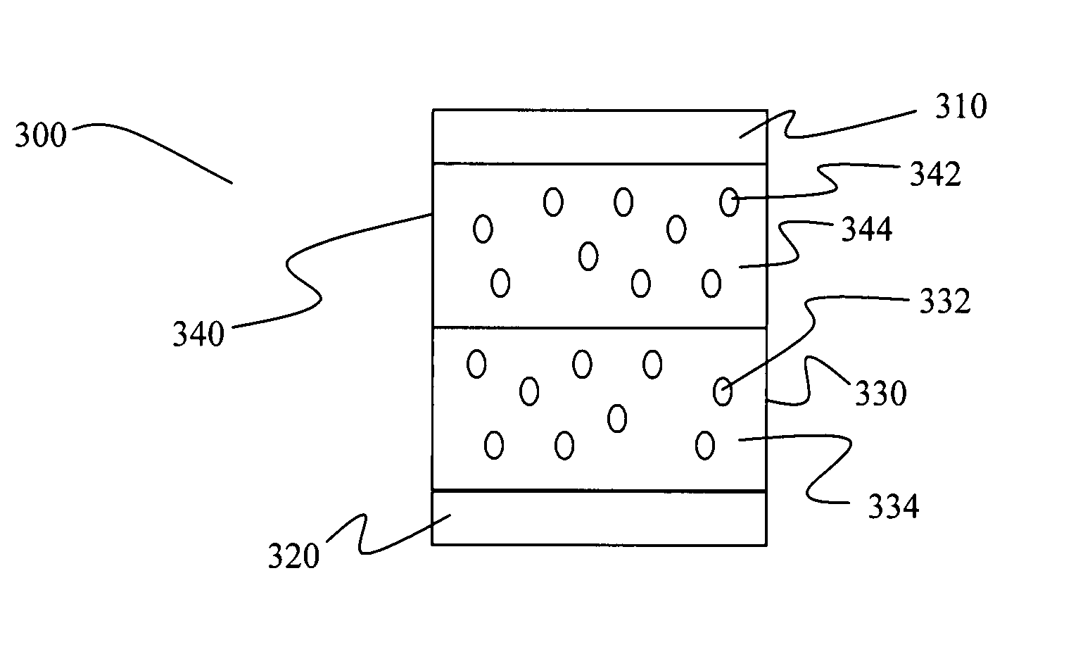
[0101] In this example, the fabrication of electronic devices in accordance with the instant invention is described. The devices include two or more homogeneous and / or heterogeneous layers in the active region. The device structure described in this example is a two-terminal device design having two or more layers disposed in an active region having a plug geometry, where the active region is in electrical contact with top and bottom electrodes. The different homogeneous and heterogeneous layers are deposited in a sequential fashion. The depositions occurred on a base Si wafer that included a thick SiO2 surface oxide layer disposed over a pre-fabricated nitridized refractory metal or metal alloy. A plug of nitridized refractory metal or metal alloy for a bottom electrode having a diameter of approximately 600 Å was formed in the insulating layer. As described in further detail below, one or more homogeneous or heterogeneous layers were next deposited on the plug and its surrounding ...

example 2

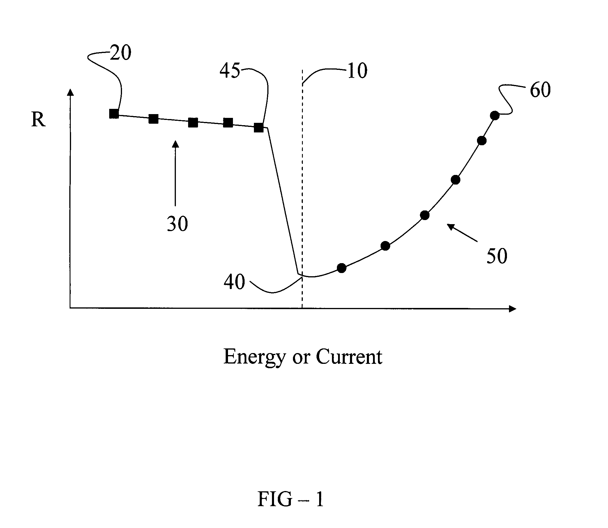
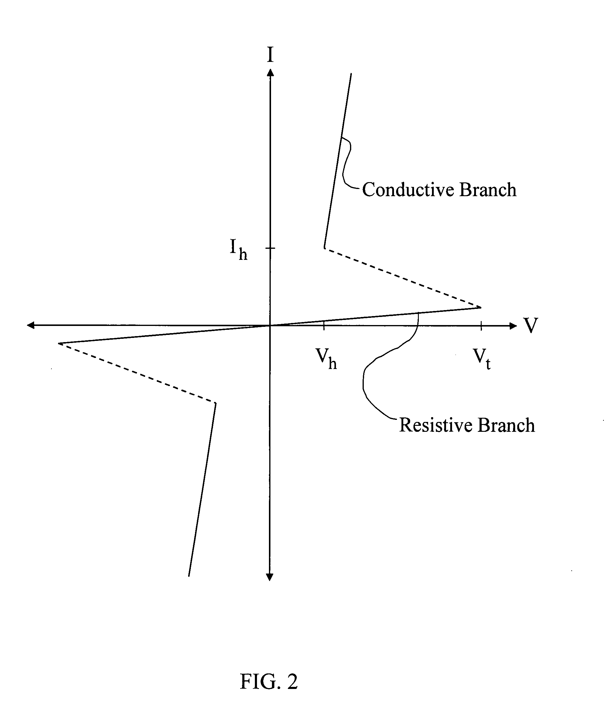
[0107] This example presents selected experimental results from the electrical testing of control device o5785. The I-V (Current-Voltage) and R-I (Resistance-Current) characteristics of the control sample are presented. The experimental results were obtained by applying voltage pulses with a pulse duration of 300 ns and various pulse amplitudes to the device. The voltage pulses were applied between the top and bottom electrodes of the device and current through the device was measured while the voltage pulse was applied. When the voltage pulse concluded, the resistance of the device was measured as well. A DC bias voltage of approximately 0.1 to 0.4 volts (V) was maintained during the read measurement. A series of voltage pulses was applied to a series-fixed resistor (Rload) in series with the electronic device under test and data was obtained for each pulse. The series of voltage pulses applied began at approximately 0.2 V and was increased in small increments up to a maximum volta...

example 3

[0113] This example presents selected experimental results from the electrical testing of device o5787. Device o5787 is an embodiment in accordance with the instant invention that includes a dual layer structure having a heterogeneous layer and a homogeneous layer. The layer in contact with the lower electrode is a 200 Å thick heterogeneous layer that includes Ge18Sb37Te45 as the operational component and 8% SiO2 as a promoter component. The layer in contact with the upper electrode is a 550 Å thick homogeneous layer of Ge2Sb2Te5. The I-V (Current-Voltage), R-I (Resistance-Current) and cycle life characteristics of device o5787 over multiple cycles were obtained as described in EXAMPLE 2 hereinabove.

[0114]FIG. 9 depicts the R-I characteristics for electronic device o5787 over several cycles of operation. The first cycle of operation is depicted as a series of data points denoted with diamond symbols that begins with the virgin state of the as-fabricated device and extends until the...


PUM


Abstract

A multi-layer chalcogenide, memory or switching device. The device includes an active region disposed between a first terminal and a second terminal. The active region includes a first layer and a second layer, where one of the layers is a heterogeneous layer that includes an operational component and a promoter component. The other layer may be a homogeneous or heterogeneous layer. In exemplary embodiments, the operational component is a chalcogenide or phase change material and the promoter component is an insulating or dielectric material. Inclusion of the promoter component provides beneficial performance characteristics such as a reduction in reset current or minimization of formation requirements.

Description

CROSS-REFERENCE TO RELATED APPLICATIONS [0001] This application is a continuation in part of U.S. patent application Ser. No. 11 / 451,913 entitled “Multi-Layer Chalcogenide Devices” filed on Jun. 13, 2006, and a continuation in part of U.S. patent application Ser. No. 11 / 301,211 entitled “Chalcogenide Devices and Materials Having Reduced Germanium or Tellerium Content” filed on Dec. 12, 2005, and a continuation in part of U.S. patent application Ser. No. 11 / 200,466 entitled “Chalcogenide Devices Incorporating Chalcogenide Materials Having Reduced Germanium or Tellerium Content” filed on Aug. 9, 2005; the disclosures of which are hereby incorporated by reference herein.FIELD OF INVENTION [0002] This invention pertains to chalcogenide materials having applications as electrical and optical memories and switches. More particularly, this invention relates to chalcogenide devices having an improved interface between a chalcogenide material and an electrical contact. Most particularly, thi...

Claims


Application Information

Patent Timeline
Patent Type & Authority Applications(United States)
IPC IPC(8): H01L47/00
CPCH01L45/06H01L45/1246H01L45/1233H01L45/1625H01L45/144H10N70/231H10N70/828H10N70/826H10N70/8828H10N70/026
Inventor SANDOVAL, REGINOCZUBATYJ, WOLODYMYRLOWREY, TYLERASANO, ISAMU
Owner OVONYX
Why Eureka
Try Eureka