Technique for low-temperature ion implantation

a technology of ion implantation and low temperature, applied in the field of semiconductor manufacturing, can solve the problems of higher dose threshold for amorphization, less than ideal shallow junctions, and more end-of-range defects, and achieve the effect of avoiding overheating the wafer

Active Publication Date: 2008-02-21
VARIAN SEMICON EQUIP ASSOC INC
View PDF10 Cites 310 Cited by
  • Summary
  • Abstract
  • Description
  • Claims
  • Application Information

AI Technical Summary

Benefits of technology

[0027]In accordance with one aspect of this particular exemplary embodiment, the method may further comprise predicting an amount of temperature increase for the wafer due to the ion implantation process and cooling the wafer based at least in part on the predicted amount of temperature increase to avoid overheating the wafer during the ion implantation process.

Problems solved by technology

As a result, a thinner amorphous layer may lead to a deeper junction depth, a less abrupt doping profile, an inadequate activation of dopants, and more end-of-range defects after anneal, all of which represent major obstacles in modern CMOS device miniaturization, especially for source-drain extension doping.
Since amorphization of the silicon occurs only when a sufficient number of the silicon atoms are displaced by beam ions, the increase of Frenkel pair annihilation at high temperatures works against the much needed amorphization process, resulting in a higher dose threshold for amorphization and therefore less than ideal shallow junctions.
Although low-temperature ion implantation has been attempted, existing approaches suffer from a number of deficiencies.
Pre-chilling an entire batch of wafers is not an easy option since each wafer will experience a different temperature increase while waiting for its turn to be implanted.
In addition, extended exposure of the vacuum chamber to the low-temperature wafers may result in icing from residual moisture.
Second, almost all existing low-temperature ion implanters cool wafers directly during ion implantation.
Apart from causing icing problems in a process chamber, direct cooling requires incorporation of cooling components (e.g., coolant pipelines, heat pumps, and additional electrical wirings) into a wafer platen.
Usually, modern wafer platens are already fairly sophisticated and very difficult to modify.
As a result, modification of an existing ion implanter or designing a new ion implanter to accommodate low-temperature processes can be prohibitively expensive while only managing to achieve marginal improvement.
Moreover, modification of a wafer platen for low-temperature ion implantation may have unwanted impact on the ion implanter's capability of performing room temperature ion implantation processes.
In addition, in-situ cooling often significantly slows down the overall ion implantation process and therefore reduces production throughput.

Method used


Image

  • Technique for low-temperature ion implantation
  • Technique for low-temperature ion implantation
  • Technique for low-temperature ion implantation

Examples


Embodiment Construction

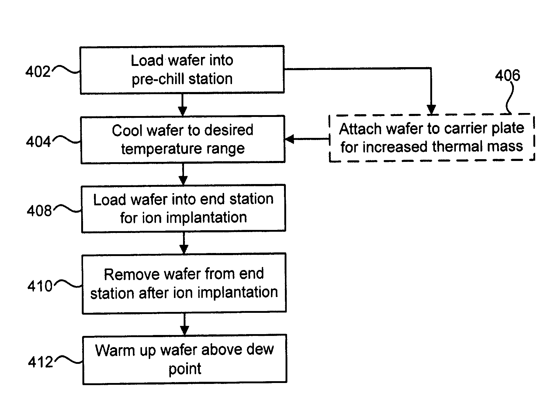
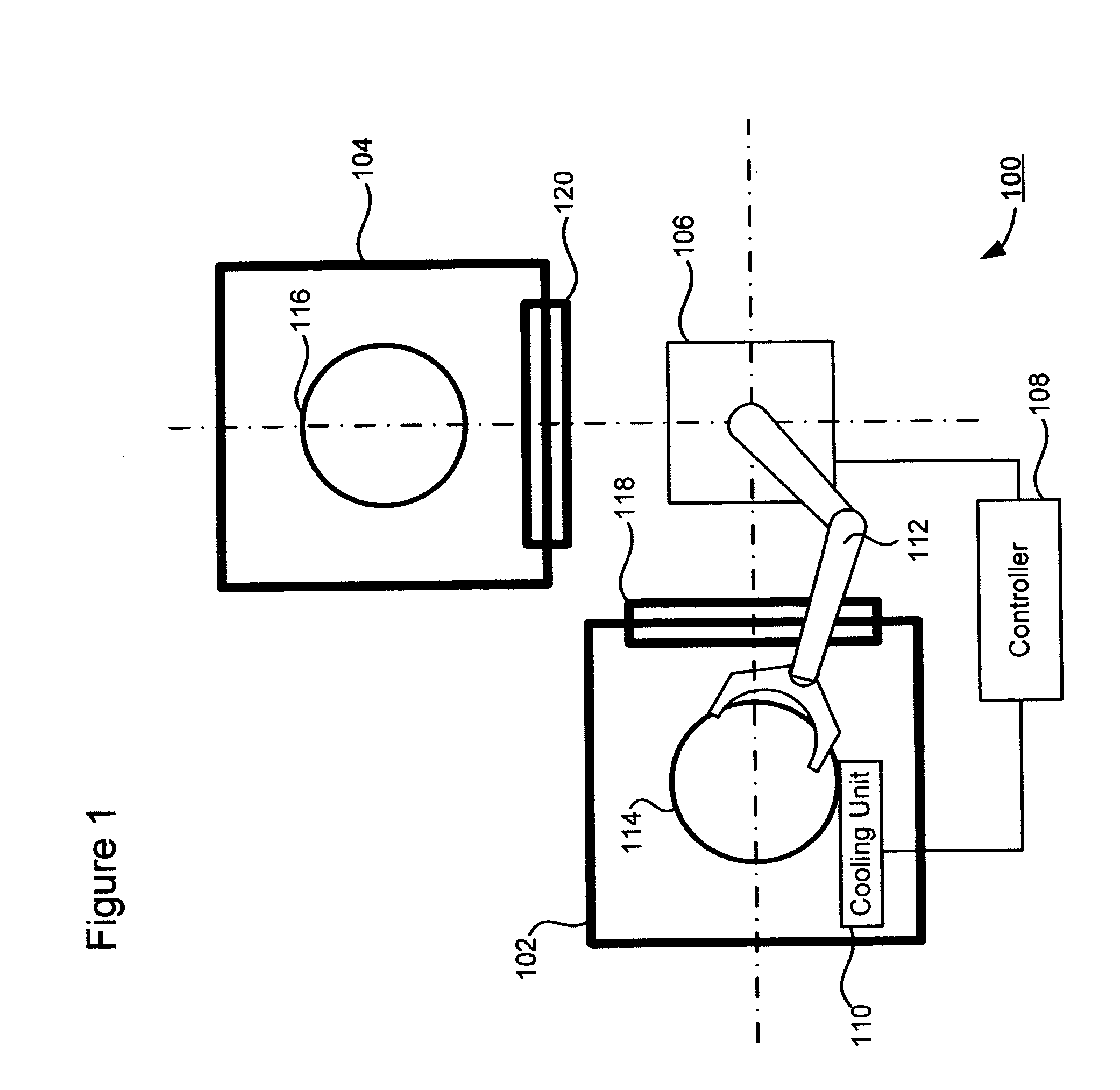
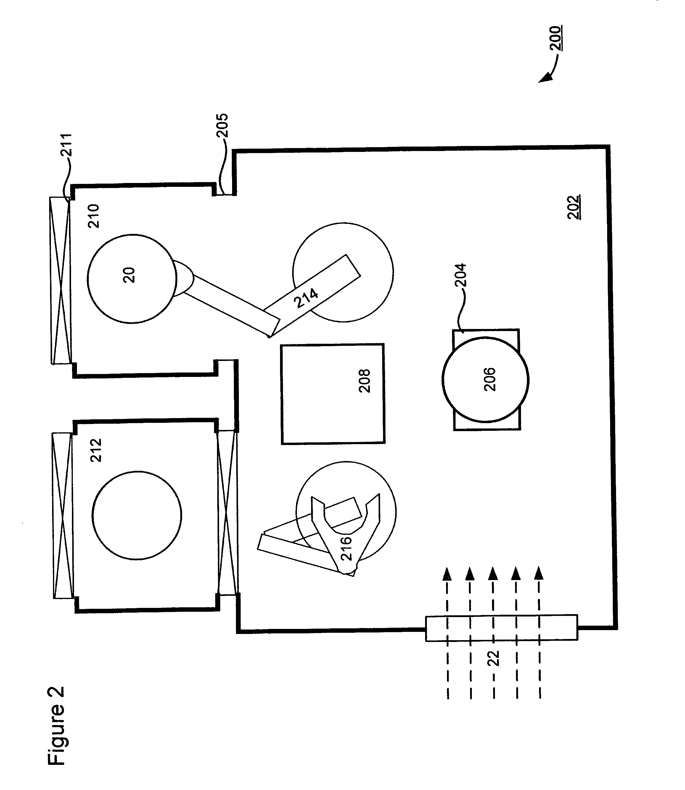
[0043]Embodiments of the present disclosure provide a technique for low-temperature ion implantation wherein a wafer may be pre-chilled to a desired temperature range before it is loaded onto a platen for ion implantation. During ion implantation, the wafer does not have to be actively or continuously cooled, and it may be thermally insulated from a wafer platen. Wafer temperature increase during ion implantation may be further mitigated by attaching the wafer to another object to achieve a larger thermal mass. The low-temperature ion implantation technique disclosed herein may be implemented for all types of ion implantation processes as well as plasma doping (PLAD) which is also referred to as plasma immersion ion implantation (PIII). Existing ion implanters may be easily modified or new ion implanters may be built to provide the pre-chilling capabilities.

[0044]As used herein, “temperature range” refers to a particular temperature value (e.g., −100° C.) or a range of temperature e...


PUM


Abstract

A technique for low-temperature ion implantation is disclosed. In one particular exemplary embodiment, the technique may be realized as an apparatus for low-temperature ion implantation. The apparatus may comprise a pre-chill station located in proximity to an end station in an ion implanter. The apparatus may also comprise a cooling mechanism within the pre-chill station. The apparatus may further comprise a loading assembly coupled to the pre-chill station and the end station. The apparatus may additionally comprise a controller in communication with the loading assembly and the cooling mechanism to coordinate loading a wafer into the pre-chill station, cooling the wafer down to a predetermined temperature range, and loading the cooled wafer into the end station where the cooled wafer undergoes an ion implantation process.

Description

FIELD OF THE DISCLOSURE[0001]The present disclosure relates generally to semiconductor manufacturing and, more particularly, to a technique for low-temperature ion implantation.BACKGROUND OF THE DISCLOSURE[0002]With continued miniaturization of semiconductor devices, there has been an increased demand for ultra-shallow junctions. For example, tremendous effort has been devoted to creating better activated, shallower, and more abrupt source-drain extension junctions to meet the needs of modern complementary metal-oxide-semiconductor (CMOS) devices.[0003]To create an abrupt, ultra-shallow junction in a crystalline silicon wafer, for example, an amorphization of the wafer surface is desirable. Generally, a relatively thick amorphous silicon layer is preferred since a thin amorphous layer can cause more significant channeling, fewer dopant atoms confined in the amorphous layer, and more interstitials residing in an end-of-range area beyond the amorphous-crystalline interface. As a resul...

Claims


Application Information

Patent Timeline
Patent Type & Authority Applications(United States)
IPC IPC(8): H01L21/00
CPCH01L21/26593H01L21/67098H01L21/67248H01L21/67213H01L21/67109H01L21/265
Inventor ENGLAND, JONATHANWALTHER, STEVEN R.MUKA, RICHARD S.BLAKE, JULIANMURPHY, PAUL J.LIEBERT, REUEL B.
Owner VARIAN SEMICON EQUIP ASSOC INC
Why Eureka
Try Eureka