Manufacturing and Use of Microperforated Substrates

a micro-perforated substrate and manufacturing technology, applied in the field of micro-perforated substrates, can solve the problems of inability to reproduce substrates with holes, and inability to produce high-quality membrane carriers. , to achieve the effect of reducing the resistance of electrical substrates, reducing the number of holes, and improving the quality of the substra

Active Publication Date: 2008-02-28
ASAHI GLASS CO LTD
View PDF7 Cites 39 Cited by
  • Summary
  • Abstract
  • Description
  • Claims
  • Application Information

AI Technical Summary

Benefits of technology

[0099]The invention also provides devices and methods for the formation of micro holes in materials usually not or difficult to machine by DEB such as glass and crystalline materials (e.g. quartz). Here the invention uses a combination of controlled heating of the substrate and CDEB to achieve holes and / or channels in the substrate. Focal heating of the substrate makes it possible to define precisely the substrate location where CDEB will take place. Varying the substrate temperature and temperature distribution provides additional means for controlling the hole and / or channel properties.
[0100]The invention further extends these CDEB methods by using alternating or modulated voltages for the hole formation. Causing the drop in electrical substrate resistance by heat contributed by dielectric losses inside the substrate material and / or electric arcs touching the substrate surface upon an application of an appropriate AC voltage, the CDEB process can be applied to materials with higher insulator—conductor transition temperatures and voltages, respectively (like glass), without an additional heat source. At the limit, the invention makes it possible to perforate substrates solely through AC voltage induced heat generation caused e.g. by electric and dielectric losses inside the substrate and electric arcs on the outside. However, (local) substrate heating preceding or being part of the initial phase of the actual CDEB process is controlled or seamlessly integrated into the CDEB as part of the invention such that at ambient temperatures usually brittle materials, such as e.g. glass, are sufficiently softened as not to break during CDEB.
[0101]An important advantage of the described CDEB methods and devices for controlled perforation is their applicability to most insulating materials. Because of the possible high aspect ratio of the produced hole structure as well as the large choice of materials, membrane carriers for e.g. Patch Clamp applications with excellent electrical as well as membrane adhesion properties can be easily, quickly and inexpensively made.

Problems solved by technology

2-200 um thick insulators, current standard materials as well as techniques used for micromachining may not provide a suitable approach to the production of inexpensive but high quality membrane carriers.
It has so far not been possible to produce high quality membrane carriers in a reproducible manner by dielectric breakdown phenomena.
More specifically it has not been possible to reproducibly produce substrates having holes in them in which holes have a diameter in the range of 0.1 um to 10 um.
It has also not been possible to introduce such holes in a manner allowing for mass production of such perforated substrates.

Method used


Image

  • Manufacturing and Use of Microperforated Substrates
  • Manufacturing and Use of Microperforated Substrates
  • Manufacturing and Use of Microperforated Substrates

Examples


Embodiment Construction

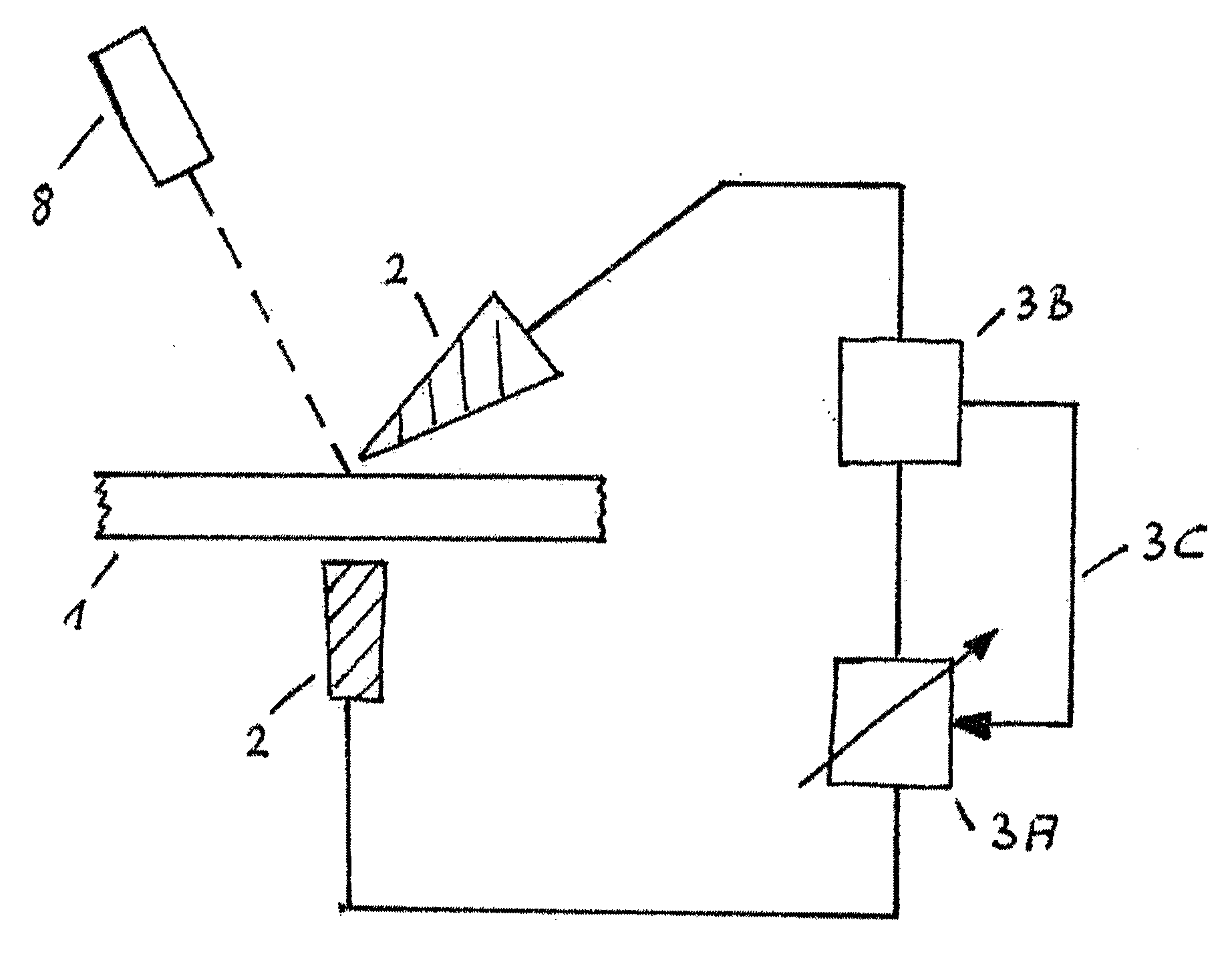
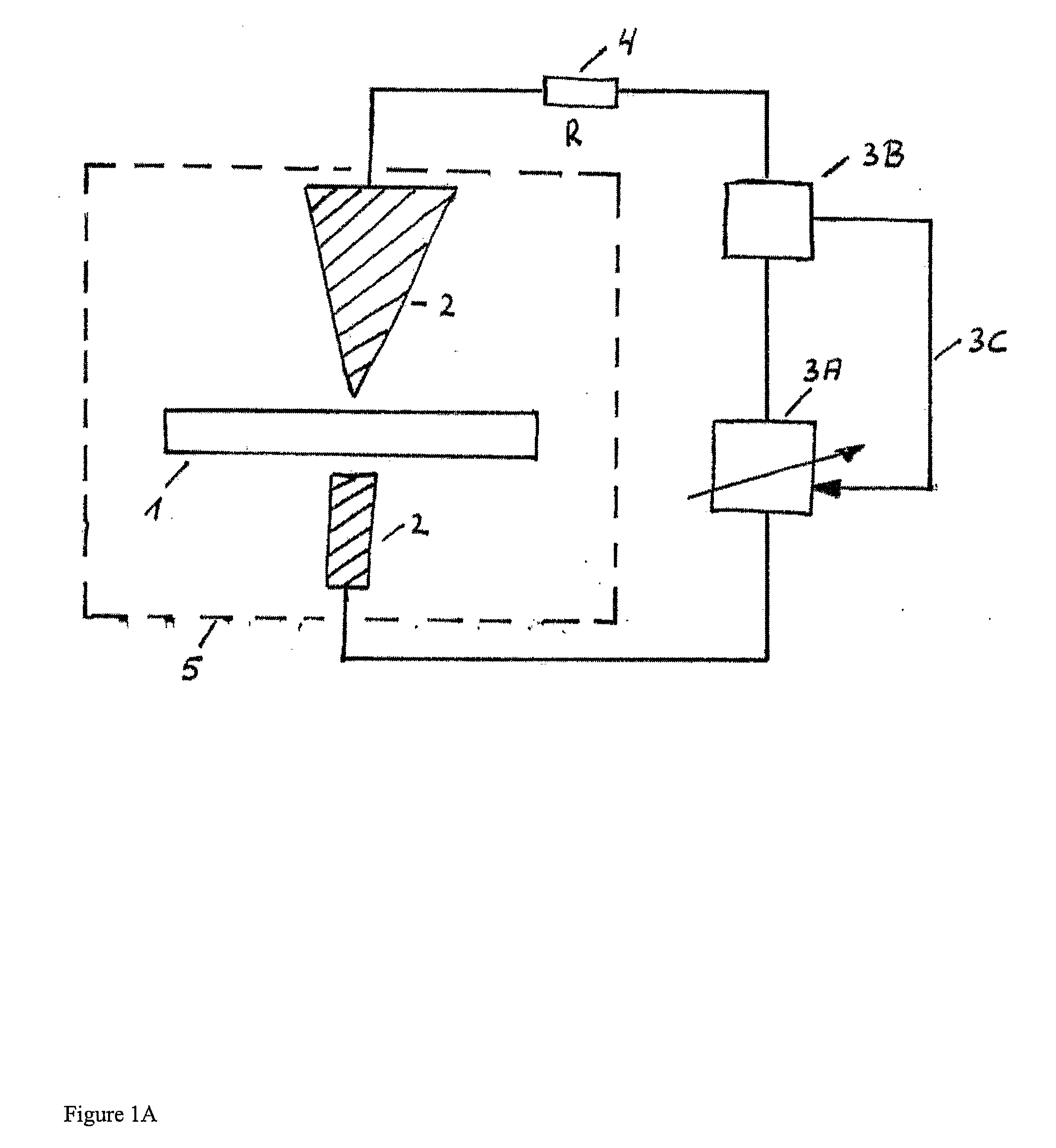
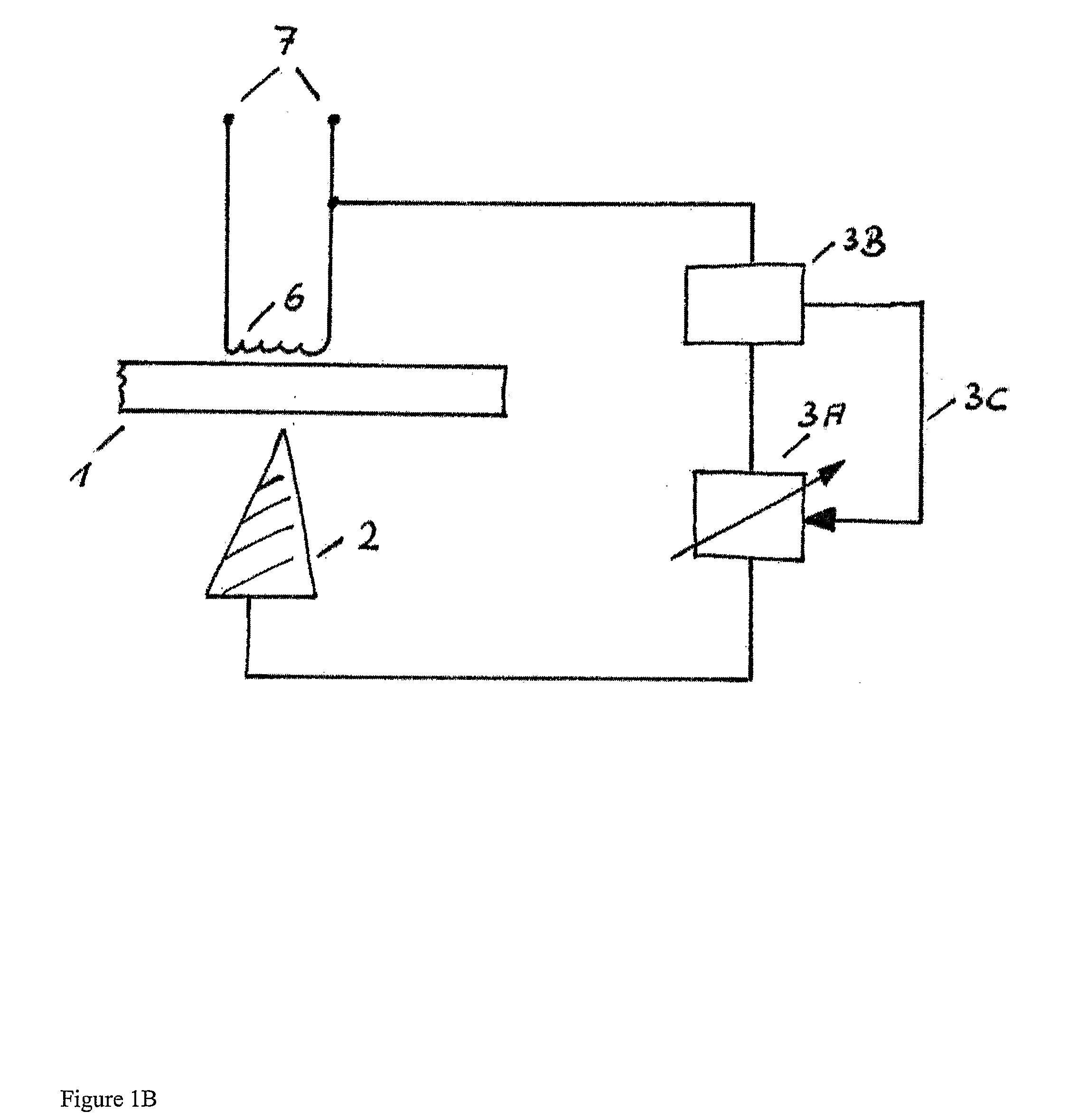
[0109]The device and methods of this invention can be used for the formation of hole and channel like structures in insulating substrates, in particular useful for electrophysiological and other measurements and set-ups where independent access to parts of biological membranes and cells is required. The terms “carrier” and “substrate” will be used synonymously and interchangeably throughout this patent application, with the term substrate referring more to the actual material to be micromachined and the term carrier indicating its actual function.

[0110]The formation of high aspect ratio hole (i.e. ‘tunnel’ or ‘channel’ like) structures in insulating or semiconducting substrates with current micromachining tools such as reactive ion etching or laser ablation is difficult, expensive and in most cases limited by size and geometry. However, for hole structures in insulating carriers used for the independent access of membrane parts, as e.g. patch clamp on a chip or BLM measurements, the...


PUM

PropertyMeasurementUnit
electrical currentaaaaaaaaaa
voltageaaaaaaaaaa
frequencyaaaaaaaaaa

Abstract

This invention relates to methods and devices for the production of micro-structured substrates and their application in natural sciences and technology, in particular in analysis and detection systems based on artificial and biological lipid membranes. The structure is preferably a hole or a cavity or channel and is obtained by spark perforation. Energy, preferably heat, is applied to the region to be structured so as to reduce the amplitude of voltage required and/or soften the material. The electrical parameters of the spark perforation are feedback-controlled.

Description

FIELD OF THE INVENTION[0001]This invention relates to methods and devices for the production of micro-structured substrates and their application in natural sciences and technology, in particular in analysis and detection systems based on artificial and biological lipid membranes.BACKGROUND OF THE INVENTION[0002]Many biological, physical or chemical analysis methods are based on lipid bilayers and biological membranes, respectively. Some of these techniques require the direct access to specific parts / patches of the membrane being usually ca. 0.1-100 um (um=10−6 meter) in diameter. Examples are electrophysiological techniques such as Patch Clamp and Black Lipid Membrane (BLM) analysis. For the standard patch clamp, such parts / patches of the membrane have been exclusively accessed by sealing a micro pipette against the cell membrane. Access to the membrane patch beneath the pipette is then directly provided through this pipette. The remaining membrane area outside the pipette is usual...

Claims


Application Information

Patent Timeline
Patent Type & Authority Applications(United States)
IPC IPC(8): B26F1/28B26D7/10
CPCB26F1/28B26D7/10
Inventor SCHMIDT, CHRISTIAN
Owner ASAHI GLASS CO LTD
Why Eureka
Try Eureka