Multiple-bank CMOS image sensor system and method

a sensor system and image sensor technology, applied in the field of multi-bank cmos image sensor system and method, can solve the problems of power-consuming external buffers/amplifiers that need to be connected, inaccuracy of analog to digital conversion, and inability to settle sample/hold circuits in the prior art, so as to increase imaging speed and reduce power consumption.

Active Publication Date: 2008-02-28
TEXAS INSTR INC
View PDF2 Cites 20 Cited by
  • Summary
  • Abstract
  • Description
  • Claims
  • Application Information

AI Technical Summary

Benefits of technology

[0012]It is an object of the invention to provide an improved system and method for providing multi-input CIS image processing integrated circuits that provide substantially increased imaging speed by, in effect, allowing parallel sampling of multiple CMOS image sensors and which also provide substantially reduced power consumption by allowing analog output signals produced by multiple CMOS image sensors to be coupled to the same input of a single ADC.

Problems solved by technology

The settling of the sample / hold circuits in the prior art have been problematic.
That in turn may cause analog to digital conversion inaccuracies.
(In some cases, costly, power-consuming external buffers / amplifiers need to be connected to the outputs of CMOS sensors in order to achieve more rapid settling.)
A problem of the prior art systems is that there cost is higher than desirable because more than one costly sample / hold circuits and ADCs are required.
Also, the prior art results in less accuracy of the digital output signals than is desired because externally generated circuit board noise is coupled to and superimposed on the analog input signals received by the inputs of the ADCs, which results in analog to digital conversion inaccuracies due to the fact that sampling timing is fixed.
However, this approach has been problematic because high speed operation usually requires correspondingly large amounts of power consumption, and also because it has typically been necessary to use costly external amplifier / buffers.
An externally generated clock signal applied as an input to an integrated circuit frequently is susceptible to outside noise influences that require clock signals be low pass filtered to reduce square wave harmonics.
This introduces delays and clock timing errors that interfere with the timing of the CIS relative to the ADCs within the multi-input CIS image processor integrated circuit chip.
With inflexible timing, inaccurate analog to digital conversion often occurs, which limits the performance of the entire imaging system.

Method used


Image

  • Multiple-bank CMOS image sensor system and method
  • Multiple-bank CMOS image sensor system and method
  • Multiple-bank CMOS image sensor system and method

Examples


Embodiment Construction

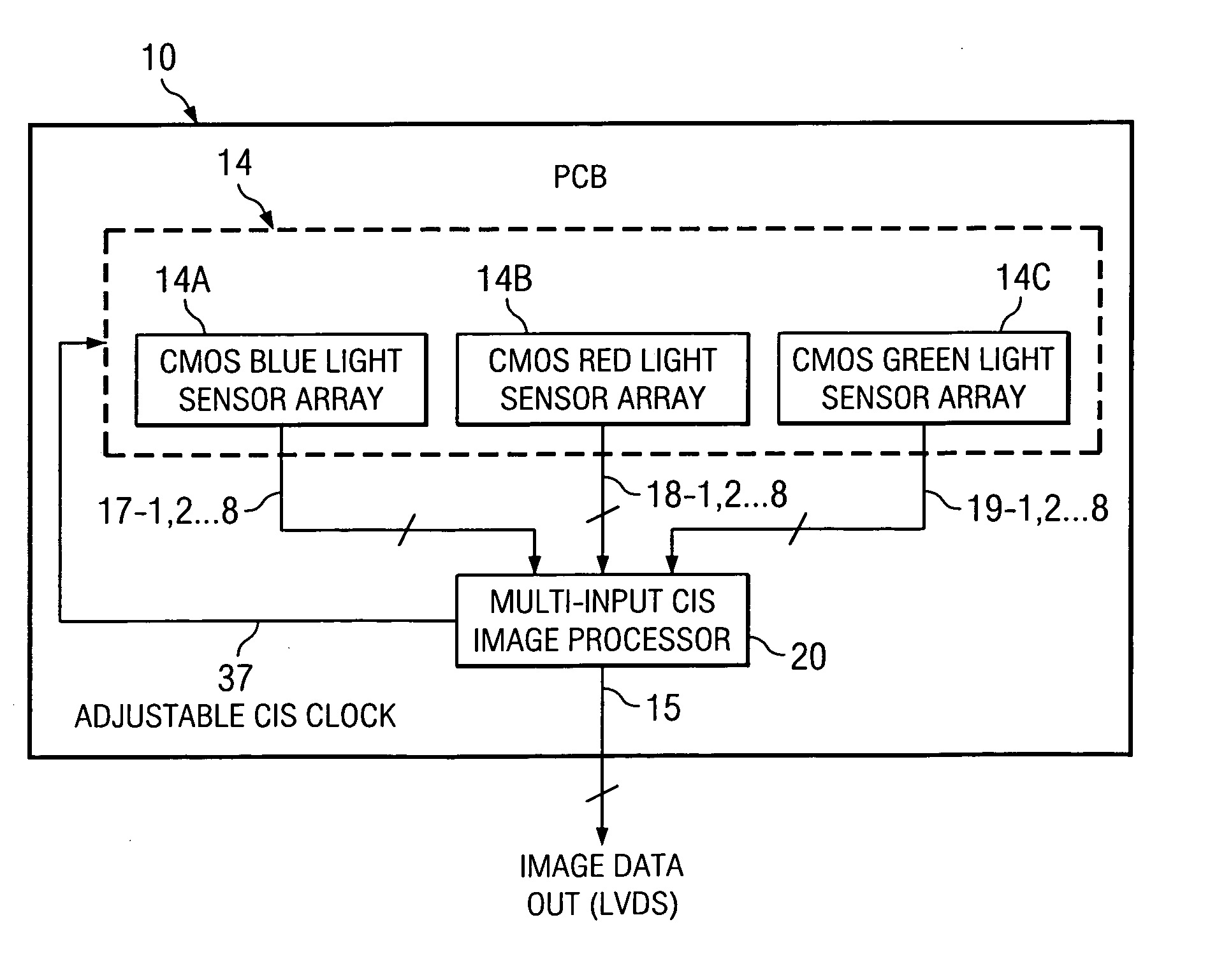
[0038]In the described embodiments of the invention, the analog output signals produced by the multiple banks of CMOS sensors are all sampled and then converted to digital equivalents within a relatively short single synchronization time frame. In order to achieve both reduced cost for the required ADCs and suitably high image processing speed, the CMOS sensors of a particular kind, e.g. blue light CMOS sensors, are arranged in banks which are alternately strobed or enabled so that the analog output signals of one bank are rapidly and sequentially coupled to the input of a single ADC while the CMOS sensors of another bank are accumulating photons and generating corresponding charge and output voltages representative of the intensity of the sensed light.

[0039]FIG. 2 shows a waveform of a clock signal CIS CLOCK which can be used to enable or strobe either a conventional CMOS sensor which produces an analog output signal representative of the ambient light intensity in response to fall...


PUM


Abstract

A CMOS image sensor system includes first and second groups of CMOS sensors each responsive to periodic first and second clock signal edges, the second clock signal edge being out-of-phase with the first clock signal edge. Output signals of the first group of CMOS sensors are coupled to a first group of sampling capacitors, respectively, by a first group of sampling switches. Then output signals of the second group of CMOS sensors are coupled to a second group of sampling capacitors, respectively, by means of a second group of sampling switches. Sampled signals on the second group of sampling capacitors to an input of an ADC, and then sampled signals on the first group of sampling capacitors are coupled to the input of the ADC by means of by multiplexing and sample/hold circuitry. A phase of at least one of the first and second clock signal edges is adjusted in response to calibration information so as to avoid circuit noise from being superimposed on sampled signals coupled to the input of the ADC.

Description

BACKGROUND OF THE INVENTION[0001]The present invention relates generally to a system and method for adjustment of clock signals in multi-input CMOS image sensor processor systems (also referred to as “CIS image systems” or “CIS image processor systems”), and more particularly to an architecture which provides an integrated circuit including multiple parallel CIS (CMOS image sensor) modules that require only a single analog to digital converter (ADC), in order to increase system imaging speed, reduce power consumption, and avoid analog-to-digital conversion inaccuracies due to externally generated noise.[0002]The CMOS image sensor samples the photons of the incoming light, and its resulting charge is converted to a voltage which subsequently is coupled to a the input of a corresponding sample / hold amplifier, which has an associated settling time. A typical CMOS image sensor (also referred to simply as a “CMOS sensor”) operates to accumulate photons and generate corresponding charge r...

Claims


Application Information

Patent Timeline
Patent Type & Authority Applications(United States)
IPC IPC(8): H03M1/12
CPCH03M1/1225H04N5/378H04N5/3742H04N5/3575H04N25/616H04N25/767H04N25/75
Inventor CORMIER, RONALD F.
Owner TEXAS INSTR INC
Why Eureka
Try Eureka