

Buried type semiconductor laser
a laser and semiconductor technology, applied in the direction of lasers, semiconductor lasers, optical resonator shapes and construction, etc., can solve the problems of deteriorating the current-light output characteristic of the laser, and achieve the effect of improving the current-light output characteristi
- Summary
- Abstract
- Description
- Claims
- Application Information
AI Technical Summary
Benefits of technology
Problems solved by technology
Method used
Image

Examples
first embodiment
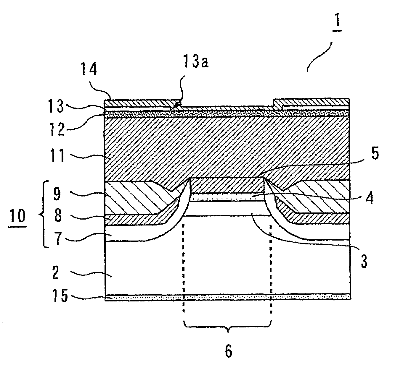
[0032]A buried type semiconductor laser according to this First Embodiment will be explained. As shown in FIG. 1, a buried type semiconductor laser 1 is made of a p-type InP substrate (hereinafter, simply referred to as a “substrate”) 2.
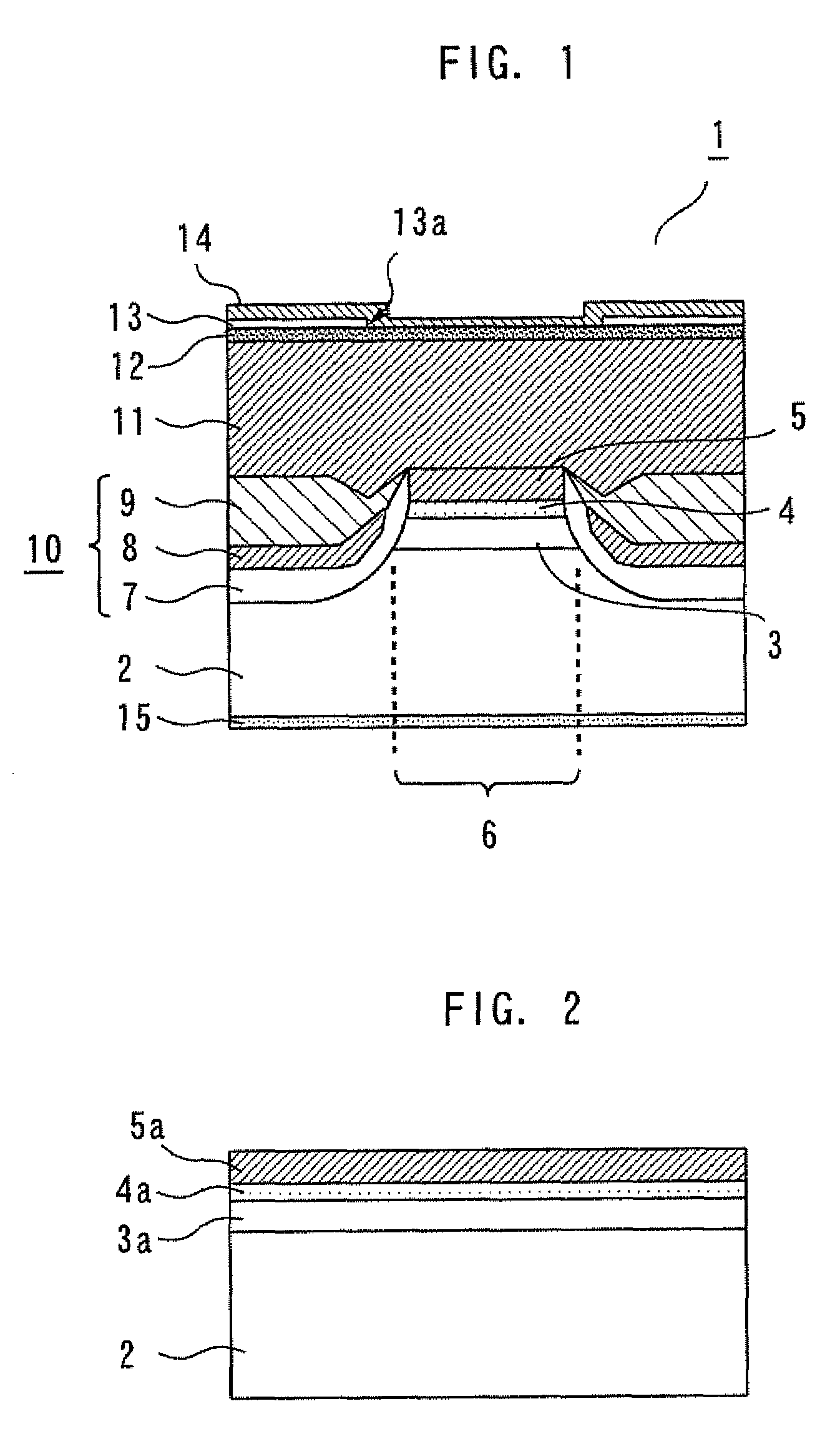
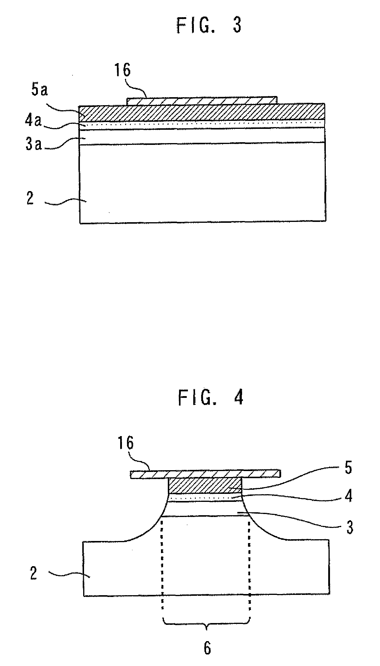
[0033]A p-type InP first clad layer 3 (carrier concentration p=1×1018 cm−3) having a fixed width is provided on the substrate 2. An AlGaInAs distorted quantum well active layer (hereinafter, simply referred to as an “active layer”) 4 which generates laser light is provided on the first clad layer 3. An n-type InP second clad layer 5 (carrier concentration n=1×1018 cm−3) is provided on the active layer 4. A ridge section 6 is made up of the first clad layer 3, active layer 4 and second clad layer 5.
[0034]A p-type InP first buried layer 7 (carrier concentration p=1×1018 cm−3) is provided so as to contact a side of the ridge section 6. An n-type InP second buried layer 8 (carrier concentration n=1×1019 cm−3) is provided so as to contact a side and top f...
second embodiment
[0048]A buried type semiconductor laser according to this Second Embodiment will be explained. Here, explanations will be focused on differences from First Embodiment.
[0049]As shown in FIG. 9, an n-type InGaAsP diffraction grating 17 (carrier concentration n=1×1018 cm−3) is provided between an active layer 4 and a second clad layer 5. The diffraction grating 17 is provided at predetermined intervals along the direction in which laser light travels and can reflect laser light of a specific wavelength. The provision of the diffraction grating 17 allows laser light in a single oscillation mode to be obtained.
[0050]Here, when p-type semiconductor is used as the diffraction grating, it is known that holes are piled up in the diffraction grating. On the other hand, since the structure shown in FIG. 9 uses n-type semiconductor as the diffraction grating, the deterioration of the current-light output characteristic can be restrained. Other aspects are the same as those in the structure show...
third embodiment
[0053]A buried type semiconductor laser according to this Third Embodiment will be explained. Here, explanations will be focused on differences from First Embodiment.
[0054]As shown in FIG. 10, an InP buried layer doped with both a p-type dopant and Fe dopant (carrier concentration p=1×1018 cm−3, carrier concentration Fe=4×1016 cm−3) is provided as a first buried layer 7a. That is, the buried type semiconductor laser in FIG. 10 is made to contain Fe in the first buried layer. Other aspects are the same as those in First Embodiment.
[0055]In the case of the structure shown in First Embodiment, the end of the first buried layer 7 and the end of the third buried layer 9 contact each other as shown in FIG. 1. Furthermore, the first buried layer 7 contains a p-type dopant such as Zn (zinc) and the third buried layer contains Fe (iron). In this case, it is known that the p-type dopant such as Zn and Fe are liable to mutual diffusion.
[0056]More specifically, most of the Fe dopant drains out ...
PUM
 Abstract
Description
Claims
Application Information