Solid-state imaging device and imaging apparatus

a technology of solid-state imaging and imaging apparatus, which is applied in the direction of radioation control devices, television systems, and scanning details of television systems, etc., can solve the problem of hardly obtaining high conversion gain in floating gates, and achieve high conversion gain, high sensitive imaging, and high conversion gain

Inactive Publication Date: 2008-03-06
SONY CORP
View PDF3 Cites 42 Cited by
  • Summary
  • Abstract
  • Description
  • Claims
  • Application Information

AI Technical Summary

Benefits of technology

[0013]In the solid-state imaging device according to an embodiment of the invention, the signal charge detection unit is arranged continuously with the channel region (for example, CCD channel), and charge transfer from the signal charge detection unit to the reset gate is performed by CCD transfer (complete transfer), therefore, the there is an advantage that the device does not have KTC noise or charge sharing noise and will be a highly sensitive imaging device. Through the signal...

Problems solved by technology

There are a problem that KTC noise and charge sharing noise exist in a FD type output unit in related arts and a problem that high conversion...

Method used


Image

  • Solid-state imaging device and imaging apparatus
  • Solid-state imaging device and imaging apparatus
  • Solid-state imaging device and imaging apparatus

Examples


first embodiment

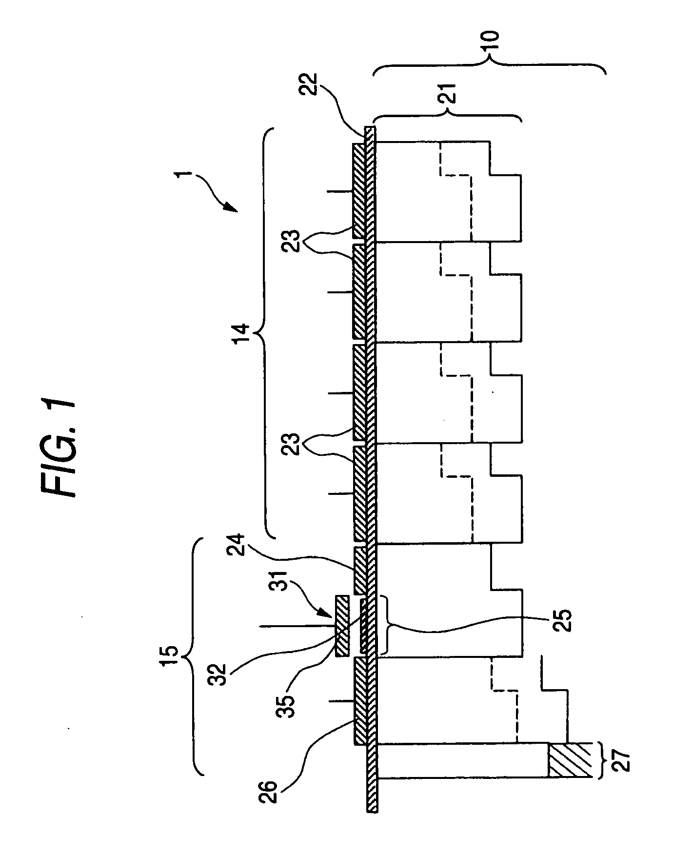
[0022]A solid-state imaging device according to an embodiment (first embodiment) of the invention will be explained with reference to configuration views of an output unit of the solid-state imaging device shown in FIG. 1 and FIG. 2 and a configuration view of the solid-state imaging device of FIG. 3.

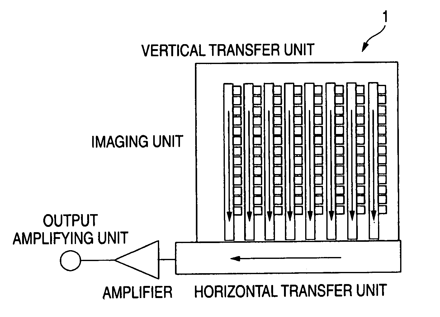
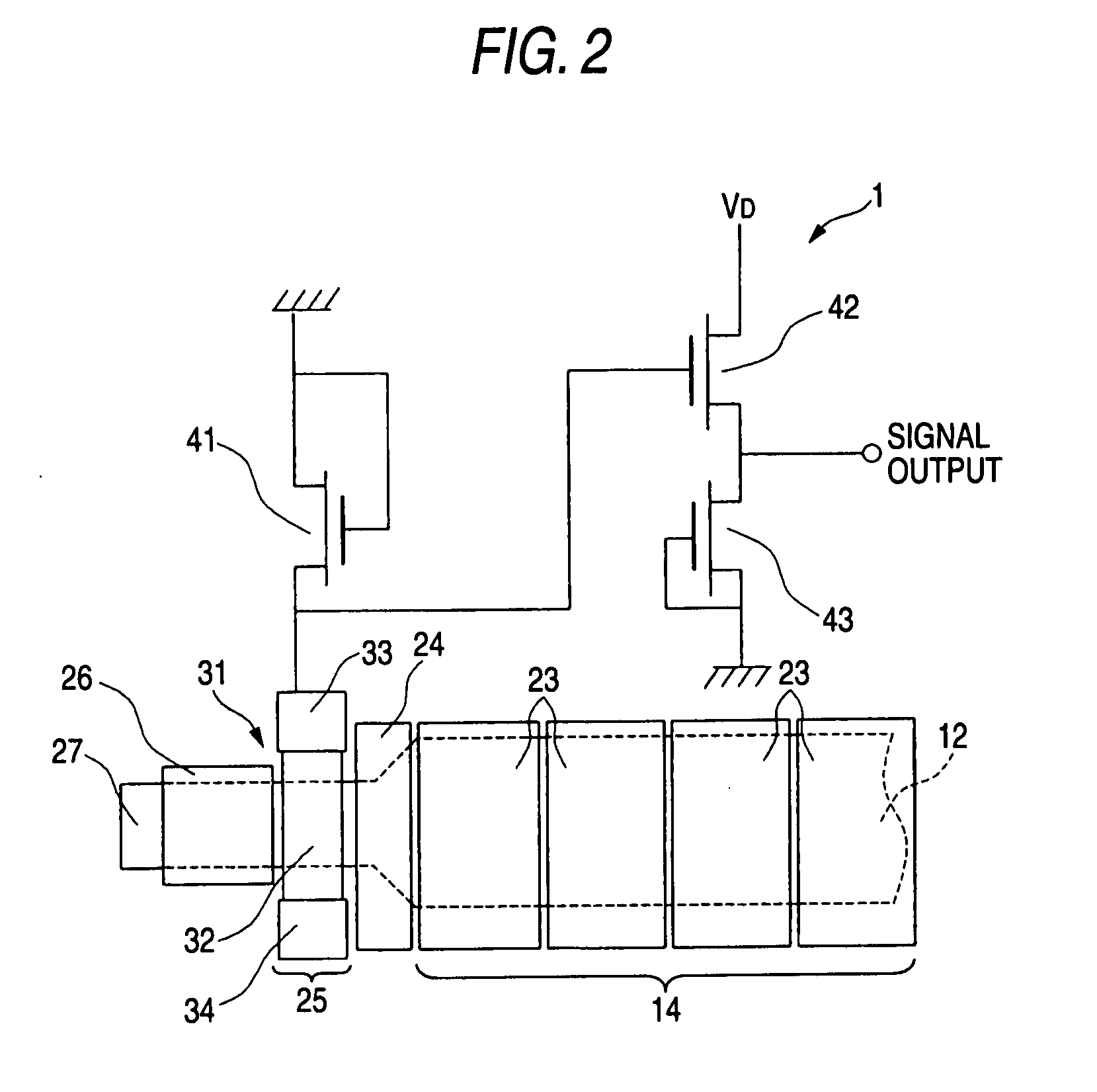
[0023]An outline of the solid-state imaging device will be explained taking a CCD solid-state imaging device as an example. As shown in FIG. 3, a solid-state imaging device (CCD solid-state imaging device) 1 includes an imaging unit 13 having photoelectric conversion units 11 photoelectrically converting incident light and vertical transfer units 12 vertically transferring charges obtained by performing photoelectric conversion at the photoelectric conversion units 11, a horizontal transfer unit 14 horizontally transferring signal charges to an output side, which have been vertically transferred, and an output unit 15 converting signal charges outputted from the horizontal transfer unit...

second embodiment

[0039]Next, a solid-state imaging device according to one embodiment (second embodiment) of the invention will be explained by a configuration plan view of an output unit of a solid-state imaging device shown in FIG. 6.

[0040]As shown in FIG. 6, a semiconductor substrate 10 is provided with the horizontal transfer unit 14 (for example, horizontal transfer CCDs) 14. The horizontal transfer unit 14 has a configuration in which transfer gates 23 are arranged on a channel region 21 formed in the semiconductor substrate 10 through an insulating film (not shown) and respective transfer gates 23 are connected to respective vertical transfer units though not shown. On an output side of the horizontal transfer unit 14 on the semiconductor substrate 10, a horizontal output gate 24, a signal charge detection unit 25, and a reset gate 26 are sequentially formed through the insulating film. Since the signal charge detection unit 25 is capable of performing nondestructive reading, for example, plu...


PUM


Abstract

A solid-state imaging device includes a signal charge detection unit converting signal charges into voltage to be outputted, which have been obtained by photoelectrically converting incident light, and in which the signal charge detection unit arranges a drive transistor having a carbon nanotube channel over a channel region between an output gate and a reset gate of a solid-state imaging device through an insulating film.

Description

CROSS REFERENCE TO RELATED APPLICATIONS[0001]The present invention contains subject matter related to Japanese Patent Application JP 2006-231505 filed in the Japanese Patent Office on Aug. 29, 2006, the entire contents of which being incorporated herein by reference.BACKGROUND OF THE INVENTION[0002]1. Field of the Invention[0003]The invention relates to a solid-state imaging device and an imaging apparatus in which a transistor using carbon nanotube is used in a charge detection circuit.[0004]2. Description of the Related Art[0005]As a signal charge detection unit of a solid-state imaging device, there is a detection unit of a floating diffusion layer (hereinafter, referred to as FD, FD is an abbreviation of “floating diffusion”), and the type is widely used as a charge detection unit of a CCD (Charge Coupled Device) type imaging device, a charge voltage conversion unit of a CMOS sensor pixel and the like. In the type, there is necessity of canceling KTC noise (thermal noise peculia...

Claims


Application Information

Patent Timeline
IPC IPC(8): H04N5/335H01L21/339H01L27/148H01L29/762H04N5/357H04N5/369H04N5/372
CPCH01L27/14837H04N3/1537H04N5/378H04N5/361H04N3/1575H04N25/63H04N25/73H04N25/75H01L27/146B82Y20/00
Inventor KANBE, HIDEO
Owner SONY CORP
Why Eureka
Try Eureka