Heat dissipation substrate for electronic device

a technology for electronic devices and heat dissipation substrates, which is applied in the direction of heat management of led devices, transportation and packaging, and metal adhesion improvement of insulation substrates, etc., can solve the problems of deterioration of high temperature of led devices, and negative impact on luminous intensity and service life, etc., to improve thermal conductivity of systems, improve the bonding with fluorine-containing polymers, and improve the effect of thermal conductivity

Inactive Publication Date: 2008-03-06
POLYTRONICS TECH
View PDF8 Cites 49 Cited by
  • Summary
  • Abstract
  • Description
  • Claims
  • Application Information

AI Technical Summary

Benefits of technology

[0011]The fluorine-containing polymer is preferably selected from poly vinylidene fluoride (PVDF) or polyethylenetetrafluoroethylene (PETFE), and has a melting point higher than 150° C., and preferably higher than 220° C. The conductive filler is selected from thermally conductive ceramic materials such as nitride and oxide. The filler can be pretreated with silane coupling agent to improve the bonding with the fluorine-containing polymer.
[0012]The fluorine-containing polymer is known for its non-stick and lack of adhesion characteristics. The most common practice to bond fluorine-containing polymer to the metal surface is to apply a tie-layer between them. However, the commonly used tie-layer for fluorine-containing polymer is not a good thermal conductive material. Even a thin layer of the tie-layer could drastically deteriorate the thermal conductivity of the system. It is a great challenge to bond fluorine-containing polymer to metal substrate and to simultaneously maintain good thermal conductivity. This invention shows the application of nodulized metal foil to bond to the highly filled thermal conductive fluoro-polymer without using tie-layer to achieve good flexibility, good thermal conductivity, and good voltage withstanding capability.
[0013]The heat dissipation substrate can be irradiated by 0-20 Mrad, so as to make the thermally conductive polymer dielectric insulating layer cross-linked and cured, and has a favorable thermally conductive and insulating effect. Further, if the thicknesses of the first metal and the second metal are designed to be smaller than 0.1 mm and 0.2 mm, respectively, and the thickness of the thermally conductive polymer dielectric insulating layer is designed to be smaller than 0.5 mm (preferably 0.3 mm), the heat dissipation substrate may pass the flexural test in which a 1 cm wide test substrate is bent to be a column with a diameter of 5 mm, and the surface neither ruptures nor cracks, thereby being applicable to a folded product.

Problems solved by technology

If the heat cannot be dissipated into the environment in time, the temperature of the LED device will become so high that the luminous intensity and service life are negatively affected.
Therefore, the heat management of the LED device attracts a lot of attention.
The common FR4 PCB cannot satisfy the heat dissipation requirement.

Method used


Image

  • Heat dissipation substrate for electronic device
  • Heat dissipation substrate for electronic device

Examples


Embodiment Construction

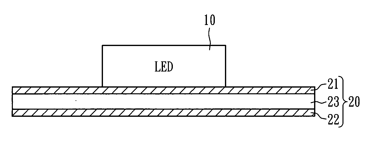
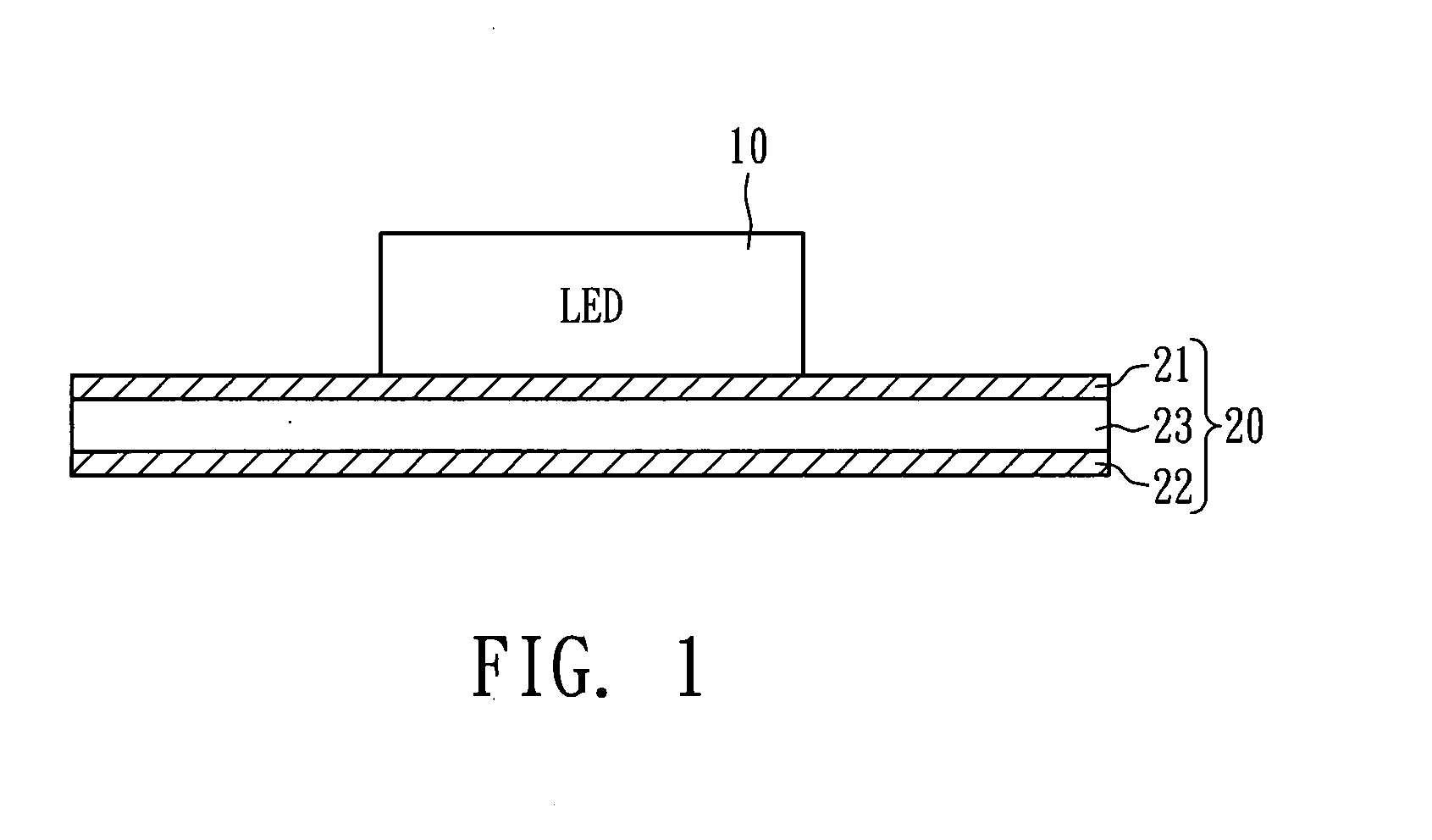
[0016]Referring to FIG. 1, an LED device 10 is carried by a heat dissipation substrate 20. The heat dissipation substrate 20 includes a first metal layer 21, a second metal layer 22, and a thermally conductive polymer dielectric insulating layer 23 stacked between the first metal layer 21 and the second metal layer 22. The LED device 10 is disposed on the surface of the first metal layer 21, and the interfaces between the first and second metal layers 21 and 22 and the thermally conductive polymer dielectric insulating layer 23 are physically contacted, wherein at least one interface is a micro-rough surface. The micro-rough surface has a plurality of nodular projections with a grain size mainly in a range of 0.1-100 μm, thereby increasing the tensile strength therebetween.

[0017]The method of fabricating the heat dissipation substrate 20 is described as follows. The feeding temperature of a batch-type blender (HAAKE-600P) is set to be 20° C. higher than the melting point (Tm) of the...


PUM

PropertyMeasurementUnit
melting pointaaaaaaaaaa
roughness Rzaaaaaaaaaa
thicknessaaaaaaaaaa

Abstract

A heat dissipation substrate for an electronic device comprises a first metal layer, a second metal layer, and a thermally conductive polymer dielectric insulating layer. A surface of the first metal layer carries the electronic device, e.g., a light-emitting diode (LED) device. The thermally conductive polymer dielectric insulating layer is stacked between the first metal layer and the second metal layer in a physical contact manner, and interfaces therebetween include at least one micro-rough surface with a roughness Rz larger than 7.0. The micro-rough surface includes a plurality of nodular projections, and the grain sizes of the nodular projections mainly are in a range of 0.1-100 μm. The heat dissipation substrate has a thermal conductivity larger than 1.0 W/m·K, and a thickness smaller than 0.5 mm, and comprises (1) a fluorine-containing polymer with a melting point higher than 150° C. and a volume percentage in a range of 30-60%, and (2) thermally conductive filler dispersed in the fluorine-containing polymer and having a volume percentage in a range of 40-70%.

Description

BACKGROUND OF THE INVENTION[0001](A) Field of the Invention[0002]The present invention relates to a heat dissipation substrate, and more particularly to a heat dissipation substrate for an electronic device.[0003](B) Description of the Related Art[0004]In recent years, white LEDs have become a very popular new product attracting widespread attention all over the world. Because white LEDs offer the advantages of small size, low power consumption, long life, and quick response speed, the problems of conventional incandescent bulbs can be solved. Therefore, the applications of LEDs in backlight sources of displays, mini-projectors, illumination, and car lamp sources are becoming increasingly important in the market.[0005]At present, Europe, the United States, Japan, and other countries have a consensus with respect to energy conservation and environmental protection, and actively develop the white LED as a new light source for illumination in this century. Currently, energy is imported...

Claims


Application Information

Patent Timeline
Patent Type & Authority Applications(United States)
IPC IPC(8): B21D39/00
CPCH05K1/034H05K1/0373H05K1/0393H05K3/384Y10T428/12472H05K2201/0209H05K2201/09309H05K2201/10106H05K2203/0307H05K2201/015
Inventor CHU, FU HUAWANG, DAVID SHAU CHEWYU, JYH MINGYANG, EN TIENCHEN, KUO HSUN
Owner POLYTRONICS TECH
Why Eureka
Try Eureka