Thin film transistor, method of fabricating active layer thereof, and liquid crystal display

Inactive Publication Date: 2008-03-06
TAIWAN TFT LCD ASSOC +6
View PDF2 Cites 20 Cited by
  • Summary
  • Abstract
  • Description
  • Claims
  • Application Information

AI Technical Summary

Benefits of technology

[0014]According to the present invention, a predetermined portion of the transistor is irradiated directly or through a mask with a light source of appropriate wavelength and energy, so as to remove organic bonding within the irradiated area of the semiconductor precursor through light-heat function, and transform the semiconductor precursor into a semiconductor material. Accordingly, direct pat

Problems solved by technology

However, since vacuum coating and photolithography processes are required for manufacturing such transistors, the cost of equipment, material, and process are substantially high.
In particular, when the size of substrate gets larger and la

Method used


Image

  • Thin film transistor, method of fabricating active layer thereof, and liquid crystal display
  • Thin film transistor, method of fabricating active layer thereof, and liquid crystal display
  • Thin film transistor, method of fabricating active layer thereof, and liquid crystal display

Examples


Example

[0025]The actual procedure of the first embodiment will be described in following example.

Example

EXAMPLE

[0026]In this example, the zinc oxide (ZnO) sol-gel solution is prepared with sol-gel. First, 100 ml 2-methoxyethanol and 3.62 ml monoethanol amine (MEA) are mixed into a mixture solution, and then 13.2 g zinc acetate is dissolved into the mixture solution. The mixture solution is stirred for 30 minutes at 60° C. to be confectioned into a ZnO precursor solution.

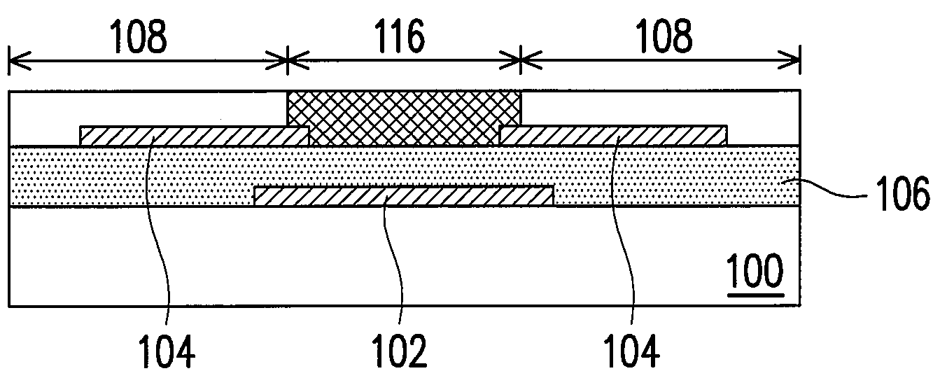
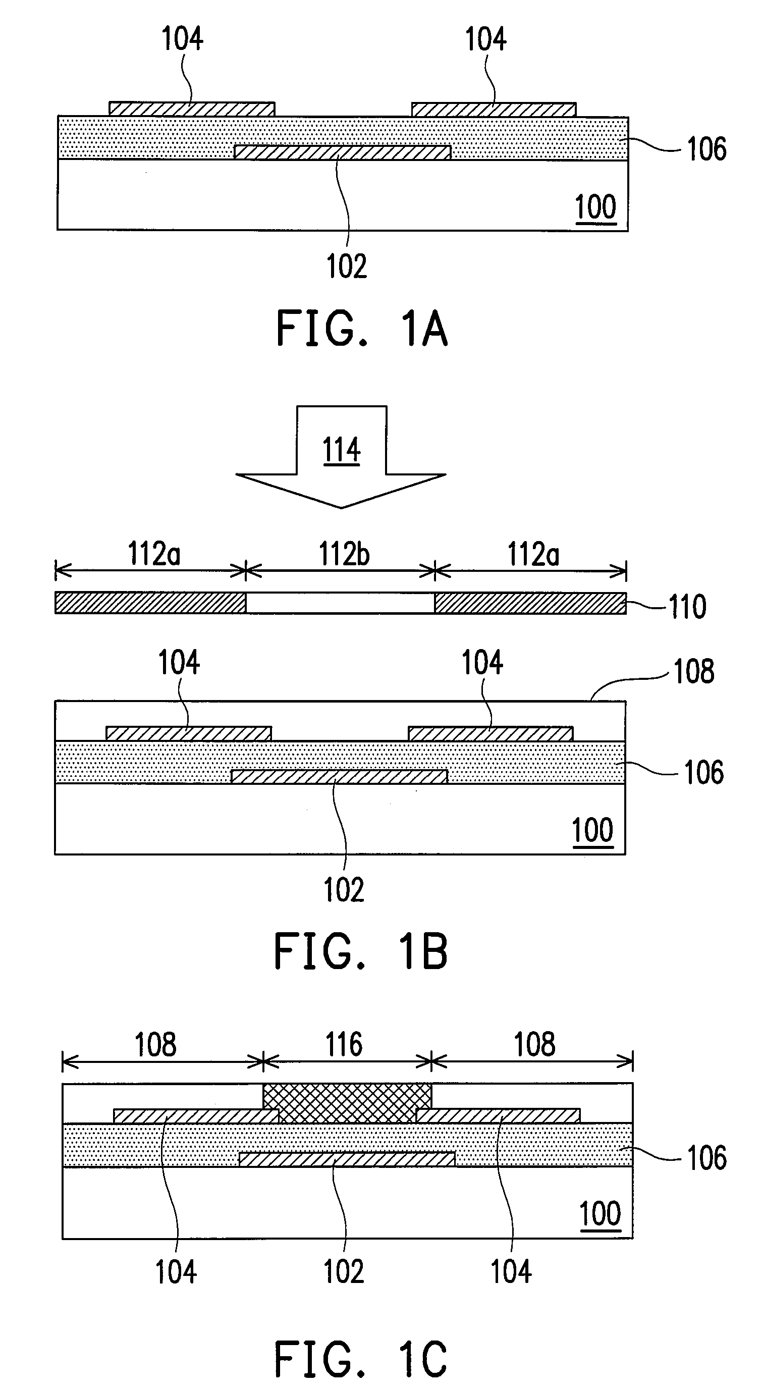
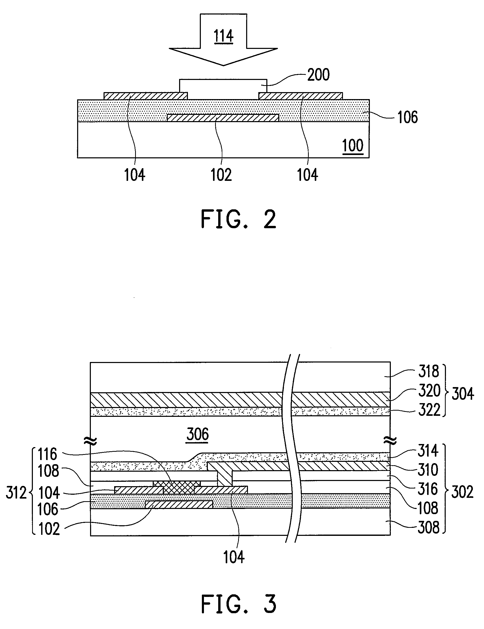
[0027]After that, the foregoing ZnO precursor solution is formed on a glass substrate through spin-coating having an ITO gate (˜1 kÅ) and a source / drain (˜1 kÅ) a layer of SiO2 has been deposited between the gate and the source / drain serving as an insulating layer (˜3 kÅ) formed thereon. Next, a step of soft baking is performed at 200° C. to transform the ZnO precursor solution into a ZnO thin film. Eventually, a KrF excimer laser having a wavelength of 248 nm is used for irradiating the ZnO thin film over the device channel (the area between the source and the drain) through a mask to remove organic bonding in the Zn...

Example

[0034]Besides being applied to the active-matrix liquid crystal display in the third embodiment, the thin film transistor in the present invention may also be applied to other types of displays or equipments such as smart card, price tag, inventory tag, solar cell, and large-area sensor array.

[0035]In summary, a liquid process is adopted along with a light source of suitable wavelength and energy in the present invention to replace the conventional thermal process. Thus, the process of the present invention can be performed in atmospheric air where only partial heating is required. Accordingly, the process is suitable for manufacturing low-cost, large-size product. Alternatively, a desired pattern may be formed, and therefore no additional photolithography or etching process is required, accordingly the process can be simplified and the fabrication cost can be effectively reduced.

[0036]It will be apparent to those skilled in the art that various modifications and variations can be m...


PUM


Abstract

A manufacturing method of an active layer of a thin film transistor is provided. The method includes following steps. First a substrate is provided, and a semiconductor precursor solution is then prepared through a liquid process. Thereafter, the semiconductor precursor solution is provided on the substrate to form a semiconductor precursor thin film. After that, a light source is used to irradiate the semiconductor precursor thin film to remove residual solvent and allow the semiconductor precursor thin film to produce semiconductor property, so as to form a semiconductor active layer.

Description

CROSS-REFERENCE TO RELATED APPLICATION[0001]This application claims the priority benefit of Taiwan application serial no. 95132538, filed Sep. 4, 2006 and Taiwan application serial no. 95141133, filed Nov. 7, 2006. All disclosure of the Taiwan applications is incorporated herein by reference.BACKGROUND OF THE INVENTION[0002]1. Field of the Invention[0003]The present invention relates to a thin film transistor and a method of fabricating an active layer thereof. More particularly, the present invention relates to a method of fabricating an active layer which can be directly performed in atmospheric air, a thin film transistor having the active layer, and a liquid crystal display.[0004]2. Description of Related Art[0005]Amorphous silicon transistor and low temperature polycrystalline transistor are the two major thin film transistors in today's active flat panel displays. However, since vacuum coating and photolithography processes are required for manufacturing such transistors, the ...

Claims


Application Information

Patent Timeline
IPC IPC(8): H01L21/84
CPCH01L29/78681H01L27/1292H01L29/7869
Inventor CHENG, HSIANG-YUANCHIANG, SHIN-CHUANLAI, SHIH-HSIANGYU, CHIN-CHIHCHUANG, BOR-CHUAN
Owner TAIWAN TFT LCD ASSOC
Why Eureka
Try Eureka