Process Solutions Containing Surfactants

Inactive Publication Date: 2008-03-13
VERSUM MATERIALS US LLC
View PDF52 Cites 43 Cited by
  • Summary
  • Abstract
  • Description
  • Claims
  • Application Information

AI Technical Summary

Benefits of technology

[0023] In yet a further aspect of the present invention, there is provided a method for avoiding a collapse of a developed pattern on the surface of a plurality of substrates and reducing photoresist line roughness comprising: providing a first substrate comprising a photoresist pattern developed upon the surface; preparing a process solution comprising from 10 ppm to about 10,000 of at least one surfactant having the formulas (I), (i), (III), (IVa), (IVb), (V), (VI), (VII), (VIII), (IXa), (IXb), (IXc), (Xa), (Xb), (Xc), or (Xd) described herein; contac

Problems solved by technology

Defects are a major limiting factor for production yield and device function, particularly when the device sizes are reduced and wafer sizes are enlarged to 300 mm.
The drive to reduce defects—thereby improving yield—presents new challenges to the manufacturing steps within the production of the semiconductor device, namely, the lithography, etching, stripping, and chemical-mechanical planarization (CMP) processes.
Pattern collapse is becoming an emerging problem in the production of semiconductor devices due to the higher aspect ratios in the new generation of devices.
Both of these approaches may require extra manufacturing steps and special equipment that are not commonly used in semiconductor device fabrication.
Foaming and bubble generation may lead to defects.
According to Domke, the addition of the “surfactant” in the developer solution did not have a consistent effect on pattern collapse.
According to Cheu

Method used


Image

  • Process Solutions Containing Surfactants
  • Process Solutions Containing Surfactants
  • Process Solutions Containing Surfactants

Examples


examples 1 through 5

Dynamic Surface Tension (DST)

[0059] Five process solutions containing acetylenic diol surfactants derived from 2,4,7,9-tetramethyl-5-decyne-4,7-diol (examples 1 through 3) or 2,5,8,11-tetramethyl-6-dodecyne-5,8-diol (examples 4 and 5) were prepared by adding 0.1 weight percent of the surfactant to deionized water under continuous stirring.

[0060] The dynamic surface tension (DST) data for each process solution was collected via the maximum bubble pressure method described in Langmuir 1986, 2, pp. 428-432. The data was collected at bubble rates that range from 0.1 bubbles / second (b / s) to 20 b / s using the Kruss BP3 bubble pressure tensiometer manufactured by Kruss, Inc. of Charlotte, N.C. The molar units of EO and PO for each example and dynamic surface tension data is provided in Table I.

[0061] The dynamic surface tension data provides information about the performance of a surfactant at conditions from near-equilibrium (0.1 b / s) to relatively high surface creation rates (20 b / s). ...

examples 5 through 7

Foaming Properties

[0062] Three process solutions containing acetylenic diol surfactants derived from 2,4,7,9-tetramethyl-5-decyne-4,7-diol (examples 5 and 6) or 2,5,8,11-tetramethyl-6-dodecyne-5,8-diol (example 7) were prepared by adding 0.1 weight percent of each surfactant to deionized water under continuous stirring.

[0063] Foaming is an undesirable side effect of surfactants in rinse solution. The foaming properties of examples 5 through 7 were examined using a procedure based upon ASTM D 1173-53, the Ross-Miles test method, and the results are provided in Table II. In this test, a 200 ml quantity of each process solution is added from an elevated foam pipette to a foam receiver containing the 50 ml of the same solution at room temperature. The Ross-Miles method stimulates the action of pouring a liquid into a cylindrical vessel containing the same liquid. The results are given in Table II. The foam height is measured at the completion of the addition (“Initial Foam Height”) an...

examples 8 through 9

Contact Angle Data

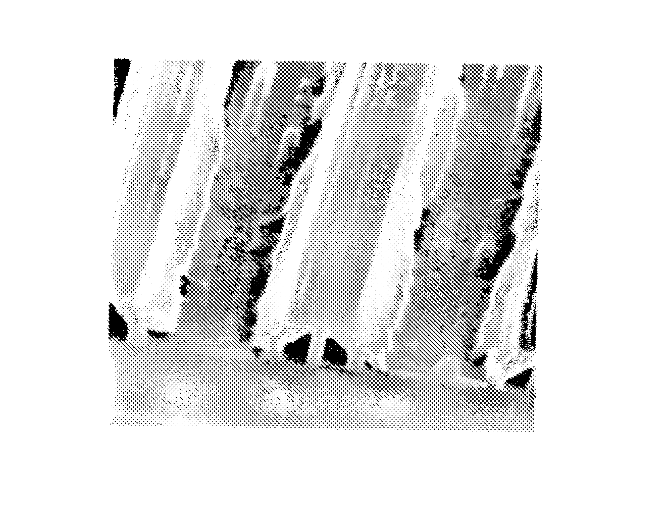
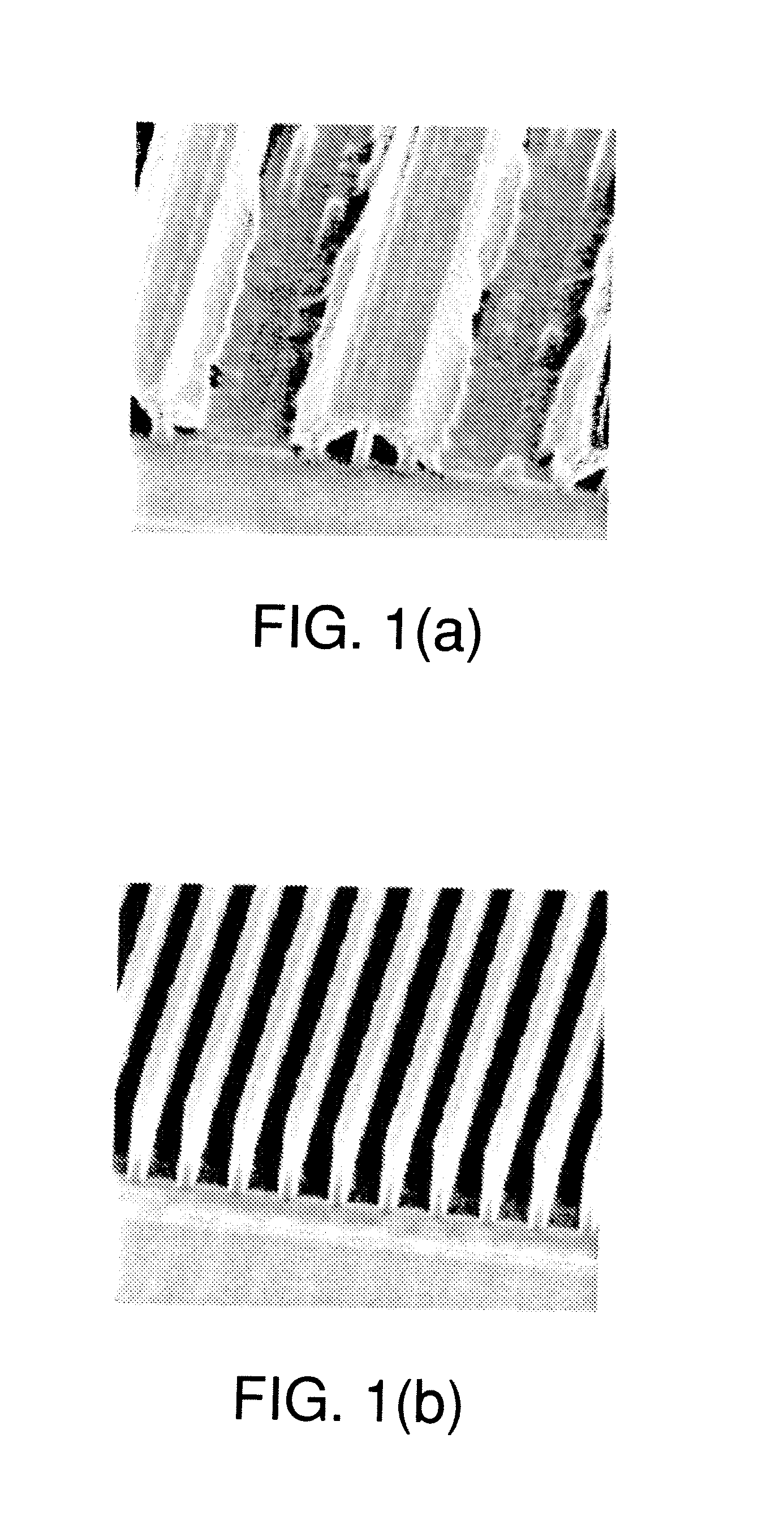
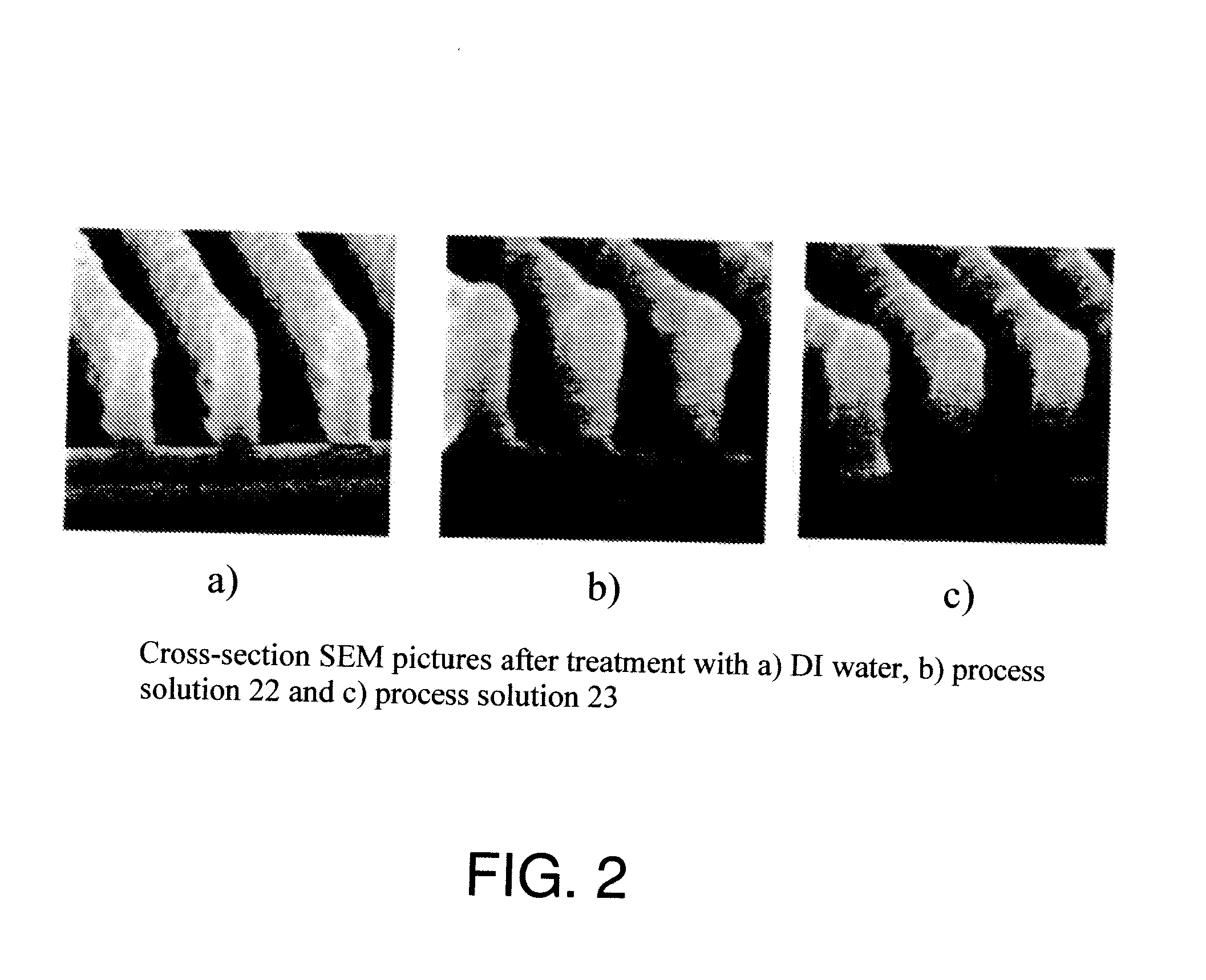
[0066] The wetting properties of process solutions containing varying amounts of surfactants derived from 2,4,7,9-tetramethyl-5-decyne-4,7-diol (examples 8a and 8b) or 2,5,8,11-tetramethyl-6-dodecyne-5,8-diol (examples 9a and 9b) and DI water as a comparison (comparative example 1) was measured on the G10 / DSA10 Kruss drop shape analyzer provided by Kruss USA of Charlotte, N.C. using the Sessile drop method. In this method, the wetting properties of a localized region on the surface of a photoresist-coated substrate are estimated by measuring the contact angle between the baseline of a droplet of aqueous developer solution and the tangent at the droplet base. A high-speed camera captured the spreading of the droplet at a speed of 2 frames per second for 2 minutes and the contact angle was measured.

[0067] Process solutions of surfactant based on 2,4,7,9-tetramethyl-5-decyne-4,7-diol and 2,5,8,11-tetramethyl-6-dodecyne-5,8-diol were prepared in the following manner....


PUM


Abstract

Process solutions comprising one or more surfactants are used to reduce the number of defects in the manufacture of semiconductor devices. In certain embodiments, the process solution may reduce post-development defects such as pattern collapse or line width roughness when employed as a rinse solution either during or after the development of the patterned photoresist layer. Also disclosed is a method for reducing the number of defects such as pattern collapse and/or line width roughness on a plurality of photoresist coated substrates employing the process solution of the present invention.

Description

CROSS-REFERENCE TO RELATED APPLICATIONS [0001] This application is a divisional of U.S. patent application Ser. No. 10 / 804,513, filed on Mar. 19, 2004, which is a continuation-in-part of U.S. patent application Ser. Nos. 10 / 218,087, filed 12 Aug. 2002, 10 / 339,709, filed 9 Jan. 2003, and 10 / 616,662 filed 10 Jul. 2003, the disclosures of which are incorporated herein by reference in their entirety.BACKGROUND OF THE INVENTION [0002] The present invention relates generally to methods for the manufacture of semiconductor devices. More specifically, the present invention relates to a method for reducing defects, particularly pattern collapse and photoresist line roughness, in semiconductor devices incurred during the manufacturing process without sacrificing throughput. [0003] Defects are a major limiting factor for production yield and device function, particularly when the device sizes are reduced and wafer sizes are enlarged to 300 mm. The term “defects”, as used herein, relates to def...

Claims


Application Information

Patent Timeline
IPC IPC(8): G03C5/00G03F7/004G03F7/09G03F7/16G03F7/30G03F7/32G03F7/38G03F7/40G03F7/42H01L21/027H01L21/304H01L21/306
CPCG03F7/0048G03F7/091G03F7/16G03F7/168G03F7/425G03F7/32G03F7/322G03F7/38G03F7/40G03F7/3021A45D34/04A45D40/26A45D2200/053A45D2200/054A45D2034/002A45D2040/0006
Inventor ZHANG, PENGCURZI, DANIELLE MEGAN KINGKARWACKI, EUGENE JOSEPH JR.BARBER, LESLIE COX
Owner VERSUM MATERIALS US LLC
Why Eureka
Try Eureka