Integrated circuit interconnection devices and methods

a technology of interconnection device and integrated circuit, which is applied in the direction of semiconductor device, semiconductor/solid-state device details, electrical apparatus, etc., can solve the problems of low electro-migration resistance, poor mechanical properties of copper-tin intermetallics, and low electrical properties, and achieve high aspect ratio, high profile features, and high stability.

Inactive Publication Date: 2008-03-27
GEORGIA TECH RES CORP
View PDF16 Cites 36 Cited by
  • Summary
  • Abstract
  • Description
  • Claims
  • Application Information

AI Technical Summary

Benefits of technology

[0010]Various embodiments of the present invention overcome the above-discussed and other drawbacks associated with conventional interconnects and interconnect fabrication methods. According to embodiments of the present invention, single metal interconnections and interconnection methods are provided. For example, electroless copper plating and annealing processes can provide substantially all-copper chip-to-substrate connections. The single metal (or conductor) can be any conductor in pure form, substantially pure form, or with specific impurities. As an example, all-copper structures can be composed of pure copper, substantially pure copper, copper with specific impurities, or copper alloys, such as copper-nickel alloys. Interconnects formed with embodiments of the present invention can have high aspect ratios to provide IC devices with high profile features (large chip-to-substrate stand-off distance).

Problems solved by technology

Solder, however, has modest electrical properties and typically has inadequate mechanical bond strength.
For example, copper-tin intermetallics have poor mechanical properties.
Another drawback associated with solder is that it has low electro-migration resistances which can affect device lifespan and performance.
While solder has provided numerous benefits for conventional IC devices, solder's chemical and physical properties may not be adequate for future integrated devices.
Thus solder properties hinder the ability to produce faster and smaller integrated devices.
For example, solder connections are limited to an aspect ratio of roughly unity so that high profile (large chip-to-substrate stand-off distance) is very difficult to obtain.
Typically used solders also have poor mechanical strength.
For example, tin and other solder-containing metals can form brittle intermetallics which fracture under high shear and normal stresses.
Due to this poor mechanical strength, underfill is generally used to support solder connections.
While providing additional mechanical strength to solder connections, underfill does create other device performance issues.
For example, underfill affects the electrical environment (poorer permittivity and conductivity loss) of IC devices.
Also, underfill and the processes used to supply underfill increase material and fabrication costs.
High temperatures are preferred to create seamless copper joining, but these high temperatures are too high for cost-effective IC devices, and the high temperatures can destroy IC device components.
Due to the solder usage, however, the electrical and mechanical limitations of solder still exist.
Further, a thin cap of solder on copper may not be able to compensate for z-axis non-uniformities (i.e., non-planar surfaces) or x, y-axis misalignment of parts.
While serving their respective purposes, these solutions are not advantageous because they still utilize solder techniques having electrical and mechanical drawbacks and also use very high temperatures not practical for IC device component manufacturing.

Method used


Image

  • Integrated circuit interconnection devices and methods
  • Integrated circuit interconnection devices and methods
  • Integrated circuit interconnection devices and methods

Examples


Embodiment Construction

[0023]Referring now to the figures, wherein like reference numerals represent like parts throughout the several views, exemplary embodiments of the present invention will be described in detail. Throughout this description, various components may be identified having specific values or parameters, however, these items are provided as exemplary embodiments. Indeed, the exemplary embodiments do not limit the various aspects and concepts of the present invention as many comparable parameters, sizes, ranges, and / or values may be implemented.

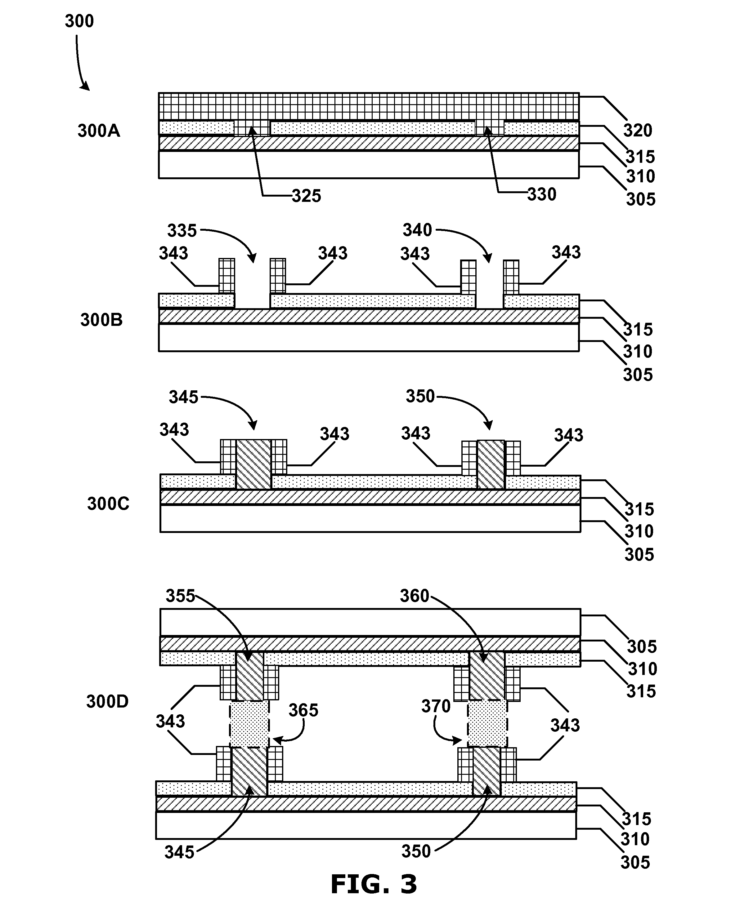
[0024]Various embodiments of the present invention provide interconnection structures and associated fabrication methods for use in IC packages. Metal pillars can be fabricated using electroplating deposition techniques and the metal pillars can be electrolessly joined at ambient temperature. Embodiments of the present invention include an electroless copper plating and annealing process to fabricate all-copper chip-to-substrate connections. Thus emb...


PUM


Abstract

Integrated circuit interconnection devices and methods are provided. An interconnection to connect components can comprise a first portion, a second portion, and a joining portion. The first portion can extend from a first component, and the first portion can be made with a single conductor. The second portion can extend from a second component, and the second portion can be made with the single conductor. The joining section can be disposed between the first portion and the second portion so that the first component and second component are interconnected to each other to form an interconnect. The joining section can be made of the single conductor so that the interconnect structure consists only of the single conductor. An interconnect can also be formed with two portions, and be formed to have a high-aspect ratio. Other embodiments are also claimed and described.

Description

TECHNICAL FIELD[0001]The various embodiments of the present invention relate generally to integrated circuit fabrication and packaging techniques, and more particularly, to interconnection devices and interconnection fabrication methods used in fabricating integrated circuit (IC) devices.BACKGROUND[0002]Solder is widely used in the electronics industry for attaching components to substrates or printed circuit boards in a flip-chip configuration. The melting point of solder, and its ability to adjust to lateral (self-alignment) and vertical (non-planar) surfaces makes it valuable in ball-grid array (BGA) packages and when utilizing epoxy substrates. Solder, however, has modest electrical properties and typically has inadequate mechanical bond strength. For example, copper-tin intermetallics have poor mechanical properties. Another drawback associated with solder is that it has low electro-migration resistances which can affect device lifespan and performance.[0003]While solder has pr...

Claims


Application Information

Patent Timeline
Patent Type & Authority Applications(United States)
IPC IPC(8): H01L23/48
CPCH01L24/10H01L2224/13099H01L24/13H01L2224/16H01L2924/01022H01L2924/01029H01L2924/0103H01L2924/01046H01L2924/01049H01L2924/01078H01L2924/01079H01L2924/01327H01L2924/14H01L2924/01005H01L2924/01006H01L2924/01024H01L2924/01033H01L2924/01047H01L2924/014H01L2224/10126H01L2924/00H01L2224/13
Inventor KOHL, PAUL A.HE, ATEOSBORN, TYLER
Owner GEORGIA TECH RES CORP
Why Eureka
Try Eureka