Light emitting device and method of making the same

Active Publication Date: 2008-03-27
TOYODA GOSEI CO LTD
View PDF12 Cites 65 Cited by
  • Summary
  • Abstract
  • Description
  • Claims
  • Application Information

AI Technical Summary

Benefits of technology

[0054] The light emitting device produced by the above embodiment (4) can be constructed such that the light emitting element is sealed by the glass with the phosphor uniformly dispersed therein. Therefore, light emitted from the light emitting element can be uniformly wavelength-converted rega

Problems solved by technology

However, the light emitting device has a first problem that the transparent resin material deteriorates due to light or heat generated from the LED element.
Especially, when the LED element is formed of a group III nitride based compound semiconductor to emit a short-wavelength light, the transparent resin material near the LED element may be yellowed due to high-energy light from the LED element and heat of the LED element itself, so that light extraction efficiency thereof lowers with time.
Thus, a second problem arises that the phosphor cannot be dispersed uniformly in the resin so that unevenness in white light discharged externally may be caused.
However, the light emitting device of JP-A-2005-011953 may cause a problem that a light emitted laterally from the LED element may be discharged externally without passing through the phosphor lay

Method used


Image

  • Light emitting device and method of making the same
  • Light emitting device and method of making the same
  • Light emitting device and method of making the same

Examples


first embodiment

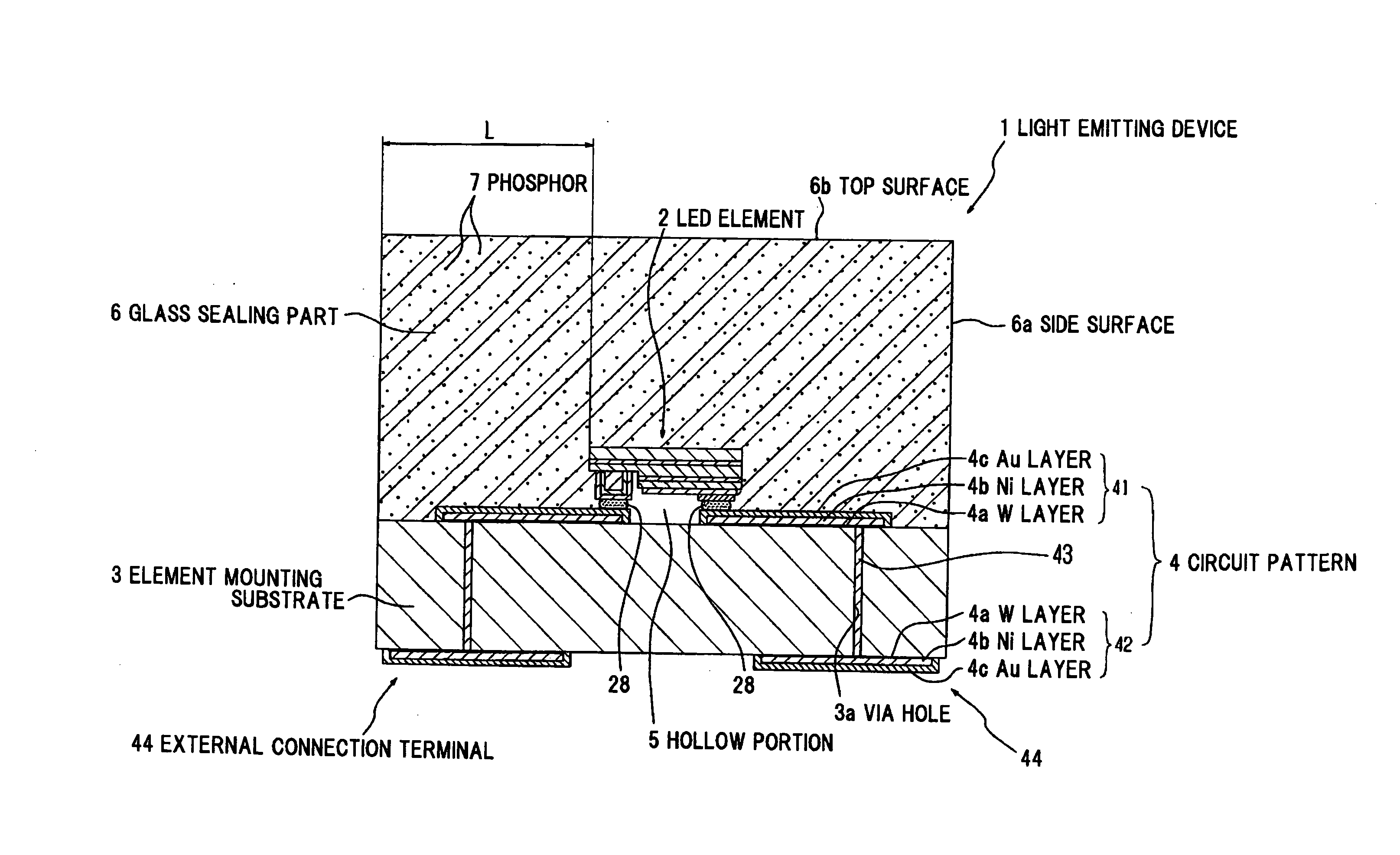
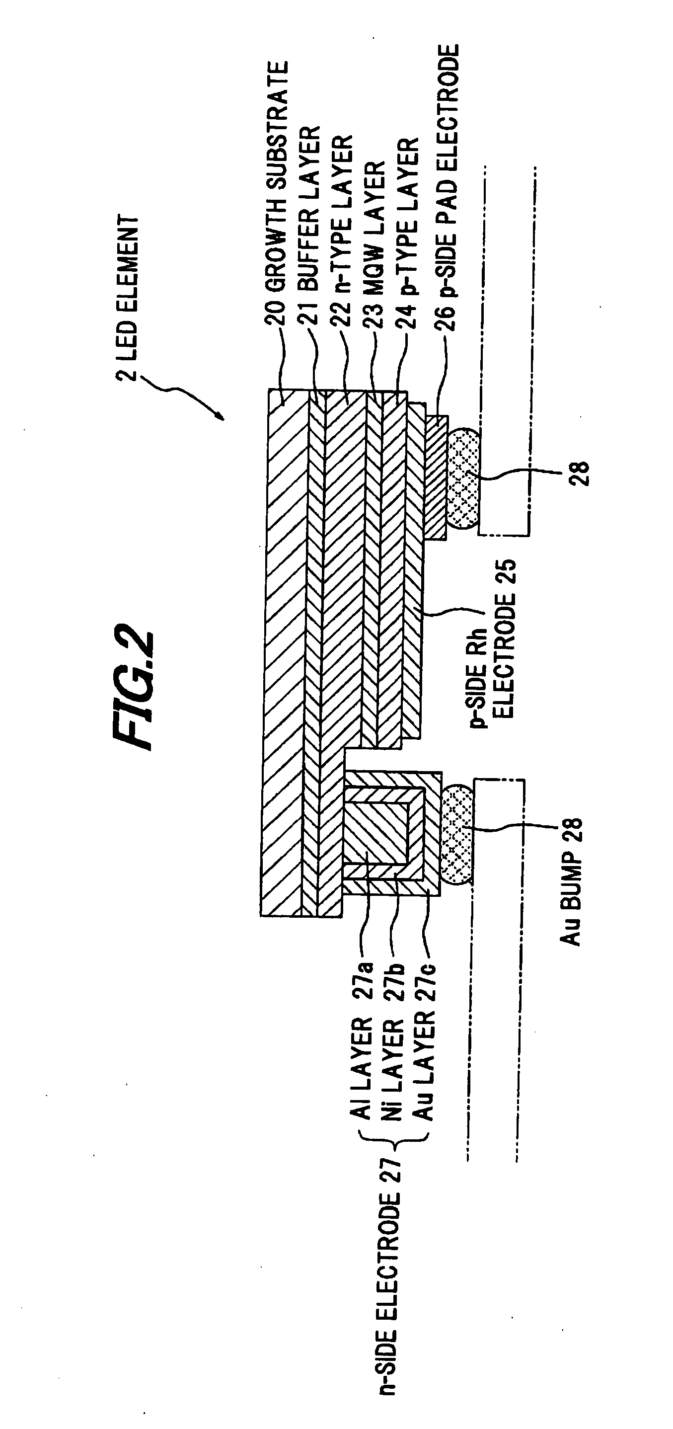
[0081] FIGS. 1 to 7 show the first preferred embodiment of the invention, where FIG. 1 is a schematic cross sectional view showing a light emitting device in the first preferred embodiment according to the invention, and FIG. 2 is a schematic cross sectional view showing an LED element in FIG. 1.

[0082] As shown in FIG. 1, the light emitting device 1 is composed of the flip-chip type LED element 2 formed of a GaN based semiconductor material, an element mounting substrate 3 to mount the LED element 2 thereon, a circuit pattern 4 formed on the element mounting substrate 3 and formed of tungsten (W)-nickel (Ni)-gold (Au), and a glass sealing part 6 to seal the LED element 2, being bonded to the element mounting substrate 3 and containing a phosphor 7 therein. A hollow portion 5 into which the sealing glass is not penetrated is formed between the LED element 2 and the element mounting substrate 3. In this embodiment, the element mounting substrate 3 and the circuit pattern 4 compose “a...

second embodiment

[0136]FIGS. 8 and 9 show a light emitting device 101 in the second preferred embodiment according to the invention. FIG. 8 is a schematic cross sectional view showing the light emitting device 101 of the second embodiment. Hereinafter, like components are indicated by the same numerals as used in the first embodiment, and duplicate explanation thereof is omitted below. Unlike the first embodiment, the second embodiment is composed such that a glass sealing part 106 is composed of two layers.

[0137] As shown in FIG. 8, the light emitting device 101 is composed of the flip-chip type LED element 2 of GaN based semiconductor material, the element mounting substrate 3 to mount the LED element 2 thereon, the circuit pattern 4 formed on the element mounting substrate 3 and formed of tungsten (W)-nickel (Ni)-gold (Au), and the glass sealing part 106 to seal the LED element 2, being bonded to the element mounting substrate 3 and containing a phosphor 7 therein. The light emitting device 101 ...

third embodiment

[0148] FIGS. 10 to 13 show a light emitting device 201 in the third preferred embodiment according to the invention. FIG. 10 is a schematic cross sectional view showing the light emitting device 201, and FIG. 11 is a schematic cross sectional view showing an LED element 202 in FIG. 10. Hereinafter, like components are indicated by the same numerals as used in the preceding embodiments, and duplicate explanation thereof is omitted below. Unlike the first embodiment, the third embodiment is composed such that a phosphor layer is provided on the circuit pattern 4 etc. of the element mounting substrate 3, and that the LED element 202 is modified from the LED element 2.

[0149] As shown in FIG. 10, the light emitting device 201 is composed of the flip-chip type LED element 202 formed of a GaN based semiconductor material, an element mounting substrate 3 to mount the LED element 202 thereon, a circuit pattern 4 formed on the element mounting substrate 3 and formed of tungsten (W)-nickel (N...


PUM


Abstract

A light emitting device has a light emitting element, a mounting portion and a sealing part. On the mounting portion, the light emitting element is mounted and a circuit pattern is formed to supply power to the light emitting element. The sealing part is formed on the mounting portion, sealing the light emitting element, and formed of a glass and a phosphor uniformly dispersed in the glass. The phosphor is adapted to emit a wavelength-converted light by being excited by a light emitted from the light emitting element.

Description

[0001] The present application is based on Japanese patent application No. 2006-247285, the entire contents of which are incorporated herein by reference. BACKGROUND OF THE INVENTION [0002] 1. Field of the Invention [0003] This invention relates to a light emitting device that a light emitting element (i.e., an LED element) is mounted on a mounting portion and sealed with glass. Also, this invention relates to a method of making the light emitting device. [0004] 2. Description of the Related Art [0005] Conventionally, a light emitting device is known in which a light emitting element such as an LED (=light emitting diode) element is sealed with a transparent resin material such as epoxy and silicone resins. In this kind of light emitting device, a light emitting device is in practical use that an ultraviolet, violet or blue LED chip is used as the light emitting element and a phosphor to be excited by a light emitted from the LED chip is mixed in the transparent resin material to ob...

Claims


Application Information

Patent Timeline
IPC IPC(8): H01J1/62H01J9/02H01L33/06H01L33/32H01L33/42H01L33/50H01L33/54H01L33/56H01L33/62
CPCH01L25/0753H01L2224/05624H01L33/56H01L33/60H01L2224/16H01L2924/01078H01L2924/01079H01L2924/09701H01L2924/01019H01L24/97H01L2224/16225H01L33/40H01L2924/351H01L33/501H01L2224/05155H01L2224/05124H01L2224/05001H01L2924/15747H01L2924/15787H01L2924/12041H01L2224/05644H01L2224/05568H01L2224/05023H01L2924/00H01L2924/00014H01L2224/06051H01L2224/06102
Inventor SUEHIRO, YOSHINOBU
Owner TOYODA GOSEI CO LTD
Why Eureka
Try Eureka