Method for forming silicon-germanium epitaxial layer

a technology of silicongermanium epitaxial layer and silicongermanium epitaxial layer, which is applied in the direction of basic electric elements, electrical apparatus, semiconductor devices, etc., can solve the problems of limiting the integration degree, affecting the yield, and limiting the performance improvement due to device miniaturization, so as to achieve uniformity and enhance throughput

Inactive Publication Date: 2008-03-27
UNITED MICROELECTRONICS CORP
View PDF6 Cites 46 Cited by
  • Summary
  • Abstract
  • Description
  • Claims
  • Application Information

AI Technical Summary

Benefits of technology

[0008]This invention provides a method for forming a SiGe epitaxial layer, wherein the uniformity of the SiGe epitaxial layer is kept while the throughput is enhanced.

Problems solved by technology

The performance improvement due to device miniaturization is thus limited.
If the device dimensions continue to reduce, a majority of the lateral area is occupied by the ohmic contacts of the source / drain regions limiting the integration degree.
However, the uniformity of a SiGe layer is usually undesirable in the prior art, which leads to the problem of pattern loading effect so that the subsequent process is difficult to control, adversely affecting the yield.
Moreover, if the SEG process for forming the SiGe epitaxial layer is not properly controlled, the SiGe epitaxial layer may grow at unassigned locations, which means a small selectivity window.
Furthermore, a low growth rate for the SiGe epitaxial layer or a low throughput may occur.
More seriously, the interface of the insulating spacer of the MOS transistor may be damaged.

Method used


Image

  • Method for forming silicon-germanium epitaxial layer
  • Method for forming silicon-germanium epitaxial layer
  • Method for forming silicon-germanium epitaxial layer

Examples


first embodiment

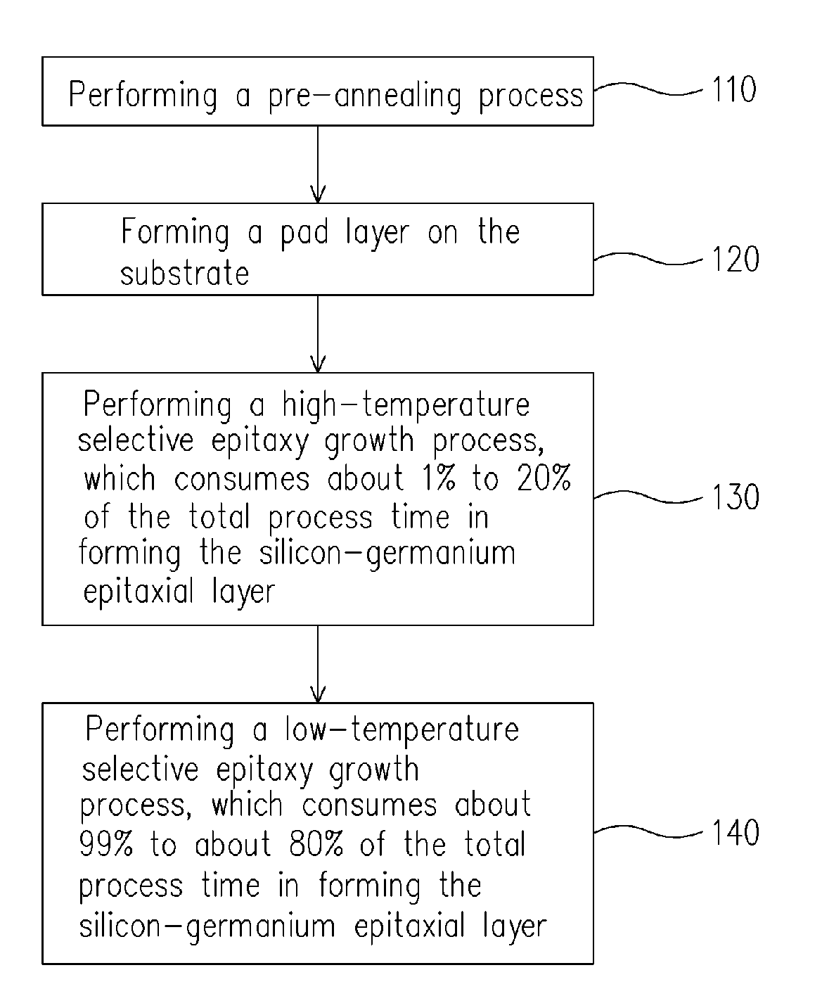
[0034]FIG. 1 is a flow chart of steps in exemplary processes that may be used in the formation of a SiGe layer according to one embodiment of this invention.

[0035]Referring to FIG. 1, in Step 110, a pre-annealing process is performed possibly at about 800° C. A pad layer is then formed on the substrate (Step 120). The pad layer and the substrate are formed with a similar material, such as, silicon.

[0036]Then, a high-temperature SEG process is conducted, consuming about 1% to 20% of the total process time for forming the entire SiGe epitaxial layer. In one embodiment, the high-temperature SEG process consumes about 1% to 15%, preferably about 1% to 10% and more preferably about 3% to 6%, of the total process time. In one embodiment, the high-temperature SEG process is conducted for about 30 seconds.

[0037]The high-temperature SEG process is performed at about 700-900° C., preferably about 750-850° C. and more preferably about 780° C.

[0038]In the above high-temperature SEG process, the...

second embodiment

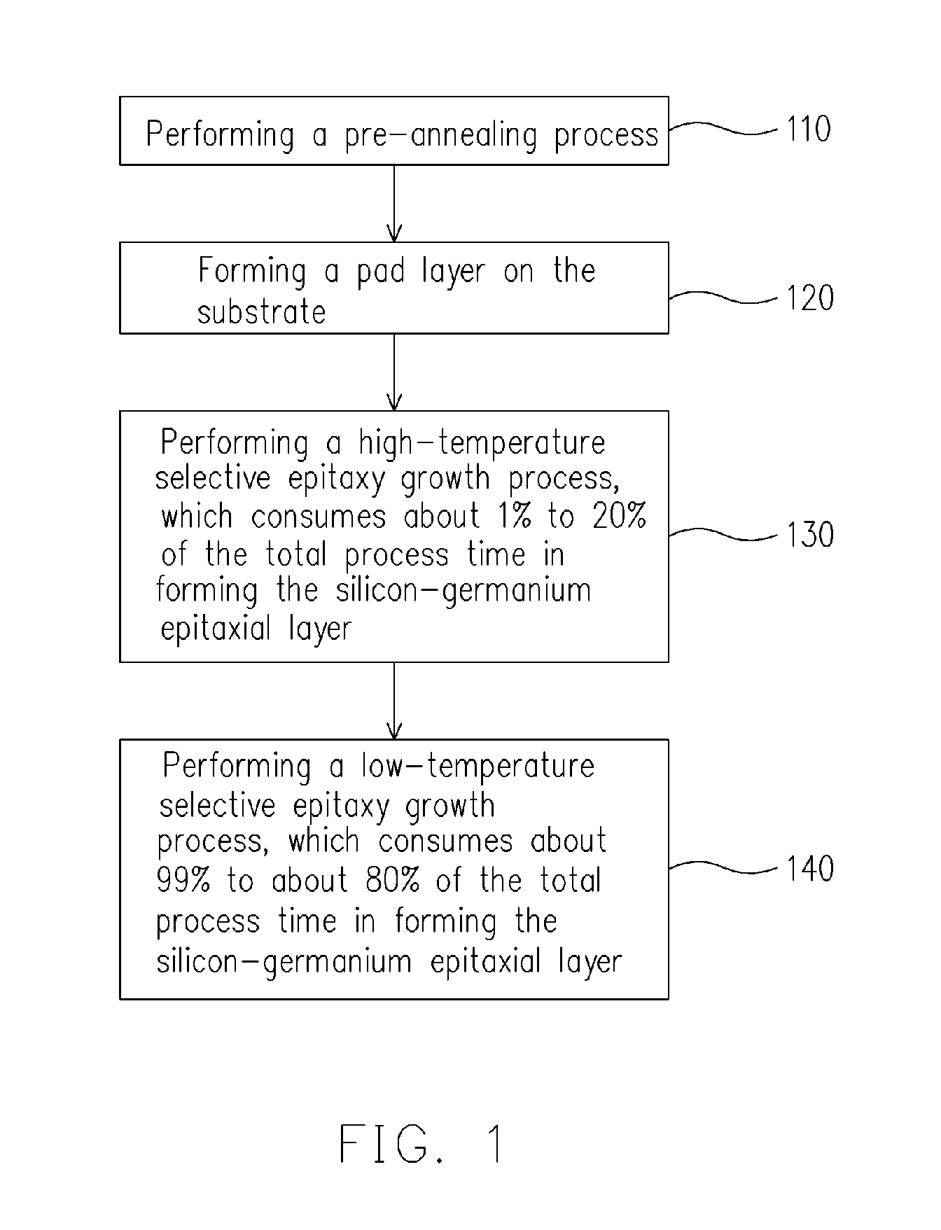
[0048]FIGS. 2A and 2B are cross-sectional views showing selected process steps for forming a SiGe epitaxial layer according to one embodiment of this invention.

[0049]Referring to FIG. 2A, the method for forming a SiGe layer of this invention is applied to the process of a PMOS transistor. An isolation structure 201 is formed in the substrate 200 and a gate structure 210 is formed on the substrate 200, wherein the substrate 200 is, for example, a silicon substrate. The isolation structure 201 includes a shallow trench isolation structure formed with silicon oxide. The gate structure 210 includes, from top to bottom, a gate dielectric layer 203 and a gate electrode 205. The material of the gate dielectric layer 203 may include silicon oxide, while that of the gate electrode 204 may include doped polysilicon, metal, metal silicide or other conductive material. The SiGe epitaxial layer is expected to form above the substrate 200 at both sides of the gate structure 210.

[0050]In one embod...

third embodiment

[0069]FIG. 4 is a flow chart of steps in exemplary processes that may be used in forming a SiGe epitaxial layer according to still another embodiment of this invention.

[0070]Referring to FIG. 4, a surface treatment is performed to the substrate in Step 410, possibly being a pre-cleaning or gas diffusion treatment. A pre-annealing process is then conducted in Step 420, possibly at a temperature of about 800° C.

[0071]In next step (430), a high-pressure SEG process is performed, consuming about 1% to 20%, preferably about 8% to 17%, of the total process time for forming the entire SiGe epitaxial layer.

[0072]The high-pressure SEG process may be performed under a pressure of about 10 Torr or higher at about 650° C. The reactant gas used includes at least a Si-containing gas and a Ge-containing gas. The Si-containing gas may include silane, disilane or dichlorosilane in a flow rate of about 50-500 sccm, preferably about 50-150 sccm. The Ge-containing gas may be germane in a flow rate of a...


PUM


Abstract

A method for forming a SiGe epitaxial layer is described. A first SEG process is performed under a first condition, consuming about 1% to 20% of the total process time for forming the SiGe epitaxial layer. Then, a second SEG process is performed under a second condition, consuming about 99% to 80% of the total process time. The first condition and the second condition include different temperatures or pressures. The first and the second SEG processes each uses a reactant gas that includes at least a Si-containing gas and a Ge-containing gas.

Description

BACKGROUND OF THE INVENTION[0001]1. Field of Invention[0002]This invention relates to a method of forming a semiconductor structure. More particularly, this invention relates to a method for forming a silicon-germanium (SiGe) epitaxial layer using a selective epitaxy growth (SEG) method.[0003]2. Description of Related Art[0004]As the IC technology enters the deep sub-micron generations, the dimensions of semiconductor devices are greatly reduced increasing the operating speed effectively. As the device dimensions are further reduced, taking a MOS transistor as an example, the parasitic capacitance and resistance of the gate and the source / drain region further increase. The performance improvement due to device miniaturization is thus limited. If the device dimensions continue to reduce, a majority of the lateral area is occupied by the ohmic contacts of the source / drain regions limiting the integration degree.[0005]Currently, the selective epitaxy growth (SEG) technique is applied t...

Claims


Application Information

Patent Timeline
Patent Type & Authority Applications(United States)
IPC IPC(8): H01L21/20H01L33/00H01L21/36
CPCH01L21/02532H01L21/0262H01L29/66636H01L29/6656H01L29/66628H01L21/02639
Inventor CHIANG, JIH-SHUNSHIH, HUNG-LINTANG, LI-YUENCHIANG, TIAN-FUFAN, MING-CHILIAO, CHIN-ICHIEN, CHIN-CHENG
Owner UNITED MICROELECTRONICS CORP
Why Eureka
Try Eureka