Printed Board And Manufacturing Method Thereof

a technology of printed boards and manufacturing methods, applied in the field of printed boards, can solve the problems of high heat generation of electronic components, such as transistors and integrated circuits, packaged on printed boards, and achieve the effects of excellent heat conductivity, excellent heat conductivity, and high efficiency

Inactive Publication Date: 2008-03-27
U AI ELECTRONICS
View PDF4 Cites 7 Cited by
  • Summary
  • Abstract
  • Description
  • Claims
  • Application Information

AI Technical Summary

Benefits of technology

[0025] According to the printed board according to Claim 1, the carbon layer that is principally made of carbon and has excellent heat conductivity is provided inside the insulator or on a surface of the insulator in a laminated form. Therefore, heat generated by the electronic component when the electronic component is energized is conducted to the carbon layer, diffused inside the carbon layer, and then radiated to the outside. As a result, the electronic component is cooled. This is advantageous in that heat generated by the electronic component when the electronic component is energized can be radiated with reliability by heat conduction to the carbon layer and heat diffusion at the carbon layer, thereby cooling the electric component with high efficiency.
[0026] The printed board according to Claim 2, in addition to the advantage demonstrated by the printed board according to Claim 1, has the heat receiving hole coupled to the carbon layer, and the heat receiving hole is filled with a metal paste or a carbon paste having excellent heat conductivity. Therefore, heat generated by the electronic component when the electronic component is energized is mainly conducted to the carbon layer via the metal paste or carbon paste filling the heat receiving hole. This is advantageous in that heat generated by the electronic component can be conducted to the carbon layer via the metal paste or carbon paste with reliability and high efficiency. As a result, the electronic component can be cooled with high efficiency.
[0027] Further the opening of the heat receiving hole is formed so as to face the back surface of the electronic component. Therefore, heat generated by the electronic component is received by the heat receiving hole (metal paste or carbon paste). This is advantageous in that heat generated by the electronic component can be conducted to the carbon layer with reliability and high efficiency, thereby further improving the cooling efficiency of the electronic component accordingly.
[0028] According to the printed board according to Claim 3, in addition to the advantage demonstrated by the printed board according to any one of claims 1 and 2, there is provided the heat radiating hole connected to the carbon layer, and the heat radiating hole is filled with the metal paste or carbon paste having excellent heat conductivity. Therefore, at least a part of heat conducted to the carbon layer from the electronic component is radiated to the outside via the metal paste or carbon paste filling the heat radiating hole. This is advantageous in that heat conducted to the carbon layer from the electronic component can be radiated from the carbon layer to the outside via the metal paste or carbon paste in the heat radiating hole with reliability and high efficiency. As a result, the electronic component can be cooled with high efficiency.
[0029] Further the opening of the heat radiating hole is provided on the surface opposite to a surface on which the electronic component is packaged or is provided in a position that does not overlap the electronic component when seen from above on an identical surface to the surface on which the electronic component is packaged. Therefore, the opening of the heat radiating hole can be formed so as not to face the back surface of the electronic component. This is advantageous in that heating of the electronic component due to radiation of heat from the heat radiating hole (metal paste or carbon paste) can be reduced, thereby further improving the cooling efficiency of the electronic component.
[0030] According to the printed board according to Claim 4, in addition to the advantage demonstrated by the printed board according to Claim 3, a heat receiving hole and a heat radiating hole are formed as one through hole in which these holes communicate to each other. Therefore, these holes can be made in one process simultaneously, for example, by drilling. This is advantageous in that there is no need to perform separate processes to make these holes, that is, the process steps are simplified, thereby allowing the processing cost to be reduced.

Problems solved by technology

Electronic components, such as a transistor and an integrated circuit (IC), packaged on a printed board generate high heat when energized.

Method used


Image

  • Printed Board And Manufacturing Method Thereof
  • Printed Board And Manufacturing Method Thereof
  • Printed Board And Manufacturing Method Thereof

Examples


first embodiment

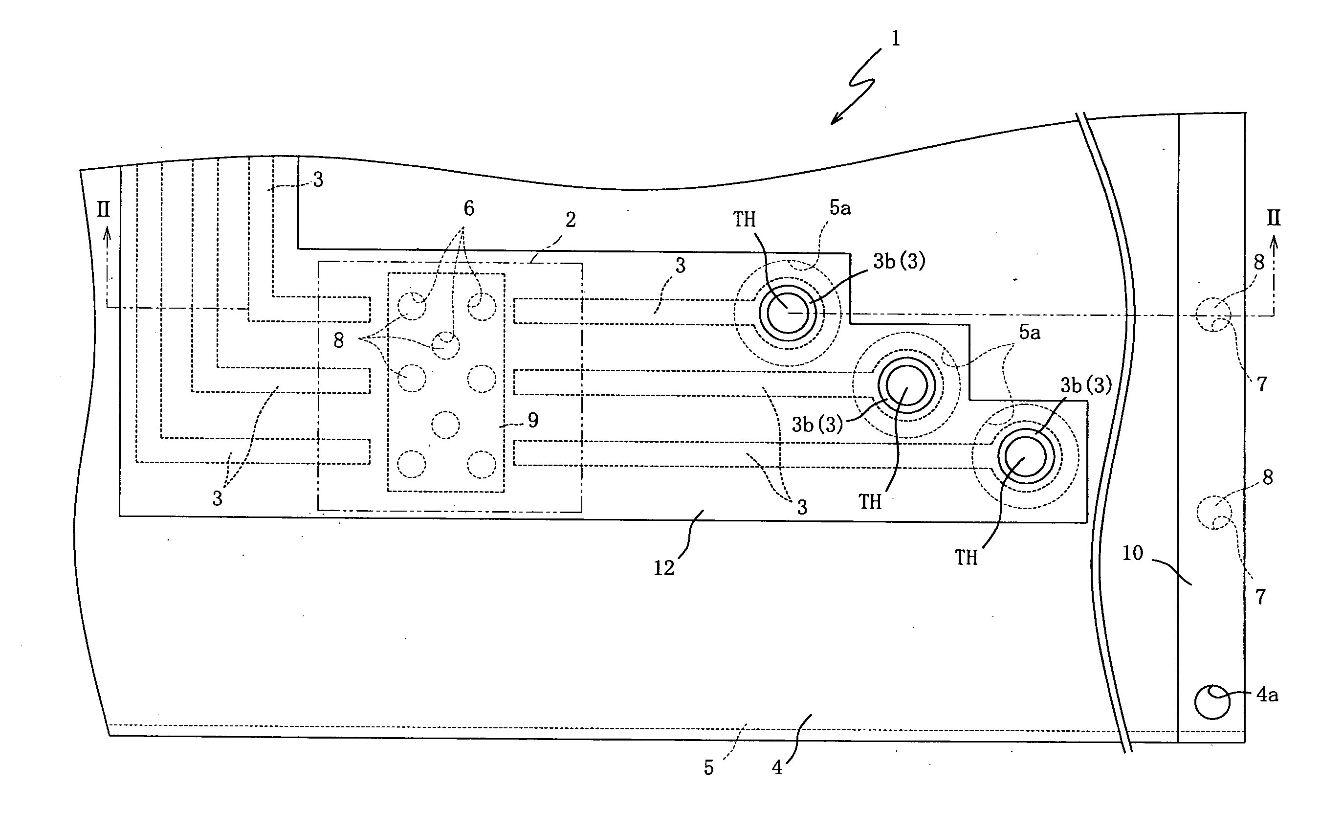
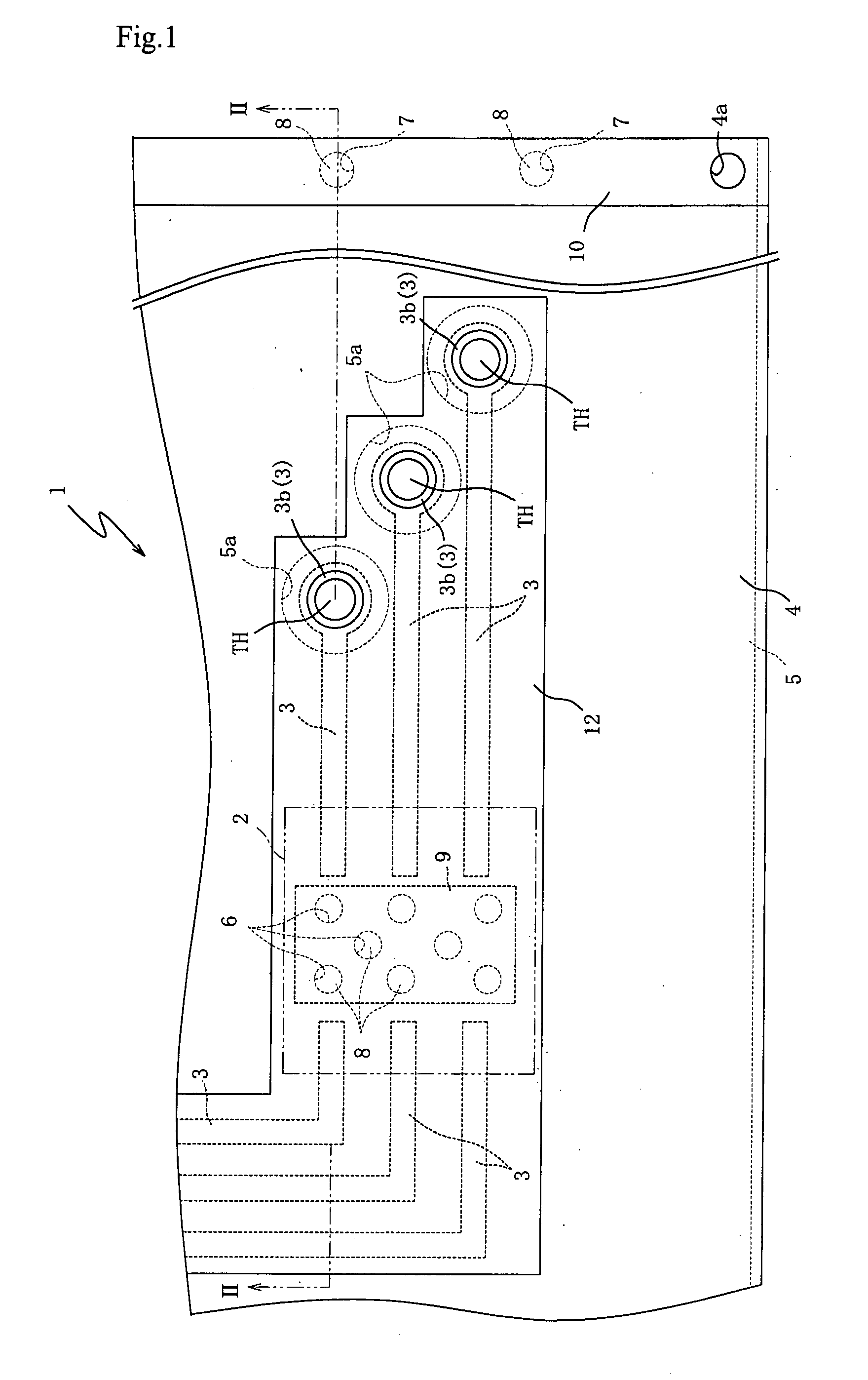
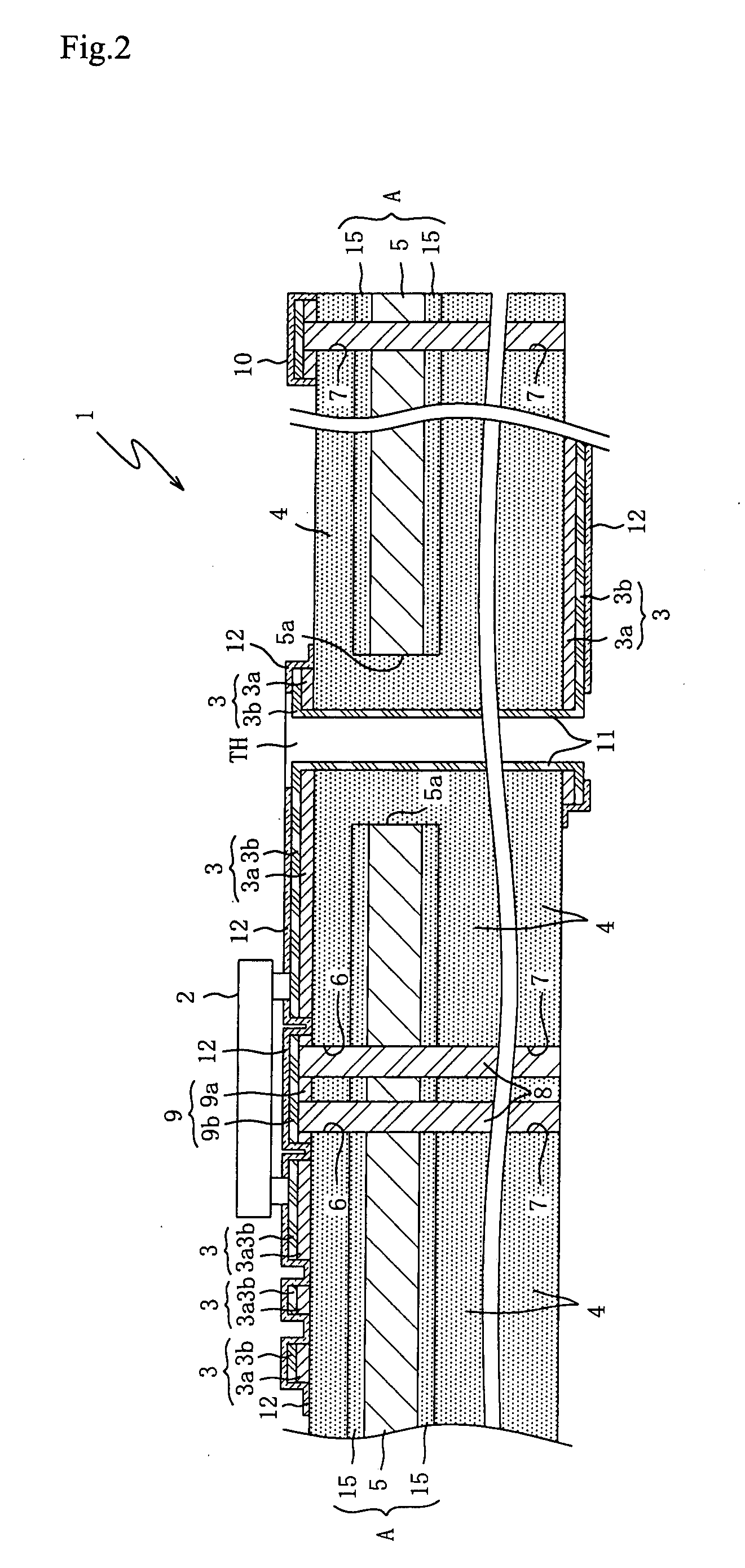
[0083] Preferred embodiments of the present invention will be described below with reference to the accompanying drawings. FIG. 1 is a top view of a printed board 1 according to the present invention. FIG. 2 is a sectional side view taken along line II-II of FIG. 1. In FIGS. 1 and 2, the printed board 1 is partially omitted. In FIG. 1, an electronic component 2 is not shown and its imaginary outline is shown using a chain double-dashed line.

[0084] The printed board 1 is, for example, a board included in an electronic device such as an engine control unit (ECU). It principally includes a plurality of electronic components 2 packaged on an upper surface thereof (toward a viewer from paper surface of FIG. 1, upper side in FIG. 2), a conductive pattern 3 for coupling these electronic components 2, an insulating board 4 on whose at least one surface (upper surface of the insulating board 4 in FIG. 2) the conductive pattern 3 is formed, and a carbon sheet 5 provided inside the insulating ...

second embodiment

[0153] Similarly in the carbon sheet 50 used in the second embodiment, the carbon containing material 50a filling the network knitted from the copper wire 50b may be made of only carbon or a mixture of carbon and other materials.

[0154] Further, in the carbon sheet 50 used in the second embodiment, the network knitted from the copper wire 50b is filled with the carbon containing material 50a. However, the member forming the network is not limited to the copper wire 50b. As a matter of course, it can be presumed that the copper wire 50b can be replaced with a material having heat conductivity. For example, a metal wire such as a silver wire may be used instead of the copper wire 50b. Further, the mesh form of the network is not limited to the knit form shown in FIG. 6. As a matter of course, it can be presumed that the network can take other mesh forms.

[0155] Further, as the method for manufacturing the printed board 1 according to the above-mentioned first embodiment, the method for...


PUM

PropertyMeasurementUnit
particle diameteraaaaaaaaaa
electrical insulatingaaaaaaaaaa
thicknessaaaaaaaaaa

Abstract

A printed board is able to cool an electronic component with high efficiency without requiring a heatsink for cooling the electronic component while preventing upsizing of the electronic device. A method for manufacturing such a printed board with high efficiency is also disclosed. Since a carbon layer principally made of carbon and having excellent heat conductivity is provided inside an insulator or on a surface of the insulator in a laminated form, heat generated by the electronic component when the electronic component is energized is conducted to the carbon layer, diffused through the carbon layer, and then radiated to the outside. Therefore, the heat generated by the electronic component can be reliably radiated by heat conduction to the carbon layer and heat diffusion through the carbon layer, thereby cooling the electric component with high efficiency.

Description

TECHNICAL FIELD [0001] The present invention relates to a printed board and a manufacturing method thereof. In particular, the invention relates to a printed board that can cool an electronic component with high efficiency without requiring a heatsink for cooling the electronic component while preventing upsizing of the electronic device, and a method for manufacturing such a printed board. BACKGROUND ART [0002] Electronic components, such as a transistor and an integrated circuit (IC), packaged on a printed board generate high heat when energized. Therefore, methods for cooling heat generated by these electronic components have been important technologies in the field of electronic devices (for example, engine control unit for an automobile (ECU)). A typical one of methods for cooling an electronic component is a method for mounting a heatsink made of a material having excellent heat conductivity on a surface of the electronic component to be heated (see Patent Document 1). There i...

Claims


Application Information

Patent Timeline
Patent Type & Authority Applications(United States)
IPC IPC(8): H01R12/00
CPCH05K1/0206H05K1/0207H05K1/056H05K3/4069Y10T29/49128H05K2201/0323H05K2203/1152Y10T29/49165H05K3/4641H05K3/42H05K3/44H05K3/46H05K7/20
Inventor TAKEZAKI, MASANORIKOMARU, MASAYUKINITTA, HARUKIYAGI, TAKAFUMIMIZUNO, YOSHIYUKI
Owner U AI ELECTRONICS
Why Eureka
Try Eureka