Thin-film semiconductor device, display, and method for manufacturing thin film semiconductor device

a thin film semiconductor and semiconductor technology, applied in the direction of semiconductor devices, basic electric elements, electrical appliances, etc., can solve the problems of high film quality, large number of film defects in silicon nitride films containing a large amount of hydrogen ions, and easy capture of contamination (mobile ions) by film defects, etc., to achieve enhanced characteristics of display elements, high blocking function, and enhanced characteristics of thin film semiconductor devices.

Inactive Publication Date: 2008-04-03
SONY CORP
View PDF2 Cites 7 Cited by
  • Summary
  • Abstract
  • Description
  • Claims
  • Application Information

AI Technical Summary

Benefits of technology

[0018]As described above, according to the embodiments of the present invention, an interlayer insulating film has a structure in which a hydrogen supply part and a blocking part are provided separately from each other. Thus, the interlayer insulating film has a high blocking function against contamination and can sufficiently repair defects in a semiconductor thin film through hydrogen supply. As a result, characteristics of a thin film semiconductor device employing this semiconductor thin film can be stably enhanced. Furthermore, in a display that includes display elements driven by thin film semiconductor elements employing this semiconductor thin film, characteristics of the display elements can be stably enhanced and thus the displaying characteristic can be enhanced.

Problems solved by technology

However, the film quality is different between the above-described silicon nitride film serving as a hydrogen ion supply source and the silicon nitride film having a blocking function against contamination.
The silicon nitride film containing a large amount of hydrogen ions includes a large number of film defects.
However, this silicon nitride film 103 includes a large number of film defects and thus contamination (mobile ion) “a” is easily trapped by the film defects.
This fixed charge makes transistor characteristics of the TFT unstable.
Furthermore, as shown in FIG. 5B, this silicon nitride film 103 is inferior in the function to block contamination because it involves a large number of film defects.
Therefore, the contamination “a” passes through the silicon nitride film 103 toward the polycrystalline silicon film 101, which makes it difficult to prevent the deterioration of element functions.
Therefore, when such a silicon nitride film is provided, it is difficult to bury hydrogen in crystalline defects in a polycrystalline silicon film although the occurrence of problems due to the contamination “a” is prevented.

Method used


Image

  • Thin-film semiconductor device, display, and method for manufacturing thin film semiconductor device
  • Thin-film semiconductor device, display, and method for manufacturing thin film semiconductor device
  • Thin-film semiconductor device, display, and method for manufacturing thin film semiconductor device

Examples


first embodiment

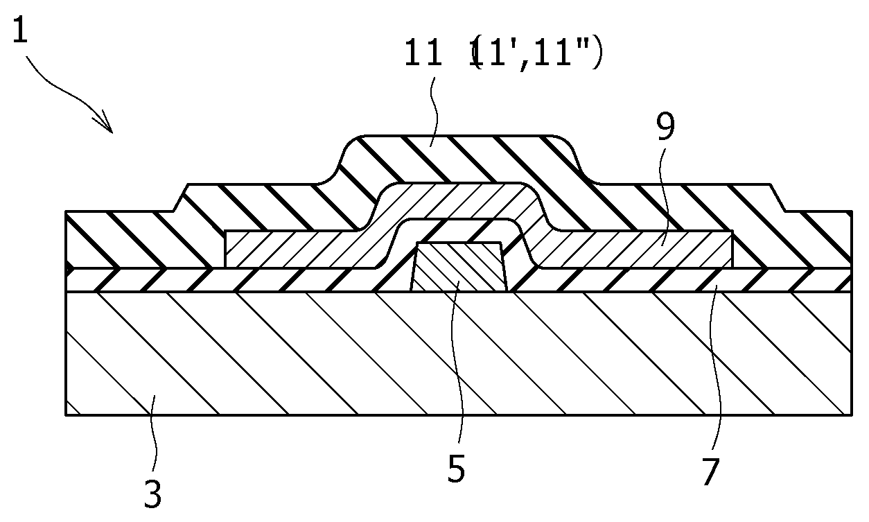
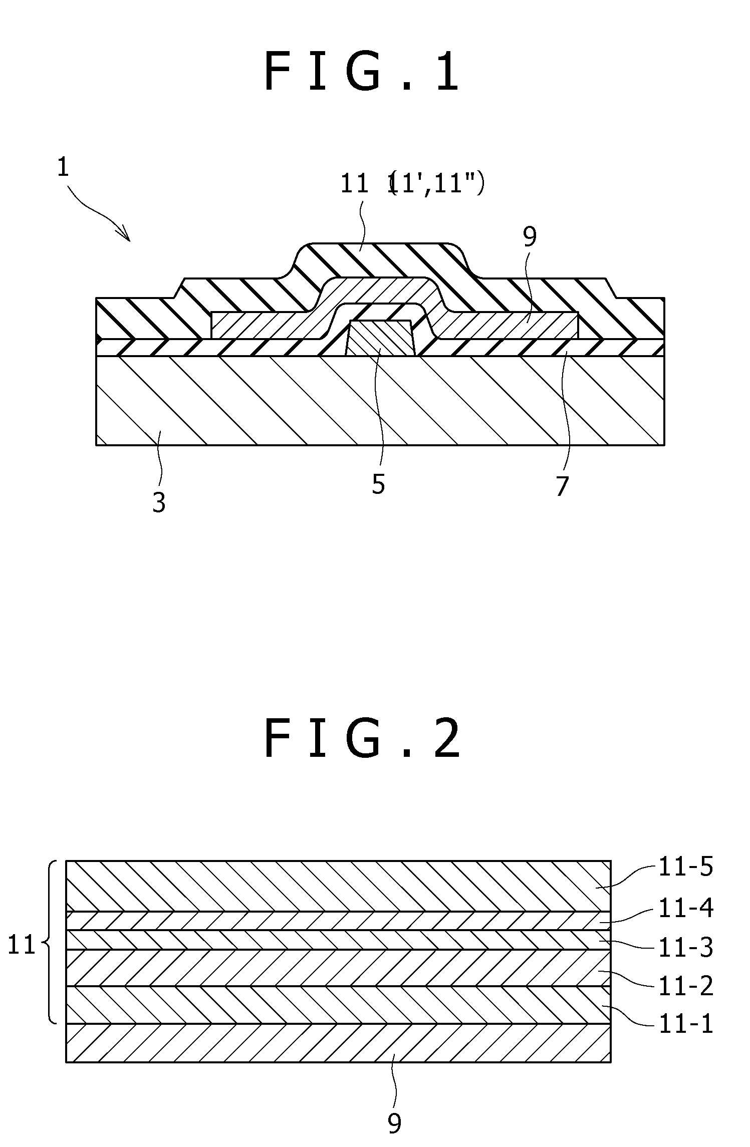
[0025]As shown in FIG. 1, a thin film semiconductor device 1 of a first embodiment of the present invention is formed as a bottom-gate thin film transistor. This thin film semiconductor device 1 includes a gate electrode 5 pattern-formed on a substrate 3, a gate insulating film 7 covering the gate electrode 5, a semiconductor thin film 9 pattern-formed on the gate insulating film 7 to overlap with the gate electrode 5, and an interlayer insulating film 11 covering the semiconductor thin film 9.

[0026]The semiconductor thin film9 is formed of a polycrystalline silicon film arising from crystallization annealing treatment by laser irradiation, and therefore includes crystalline defects. This semiconductor thin film 9 includes a channel part disposed over the gate electrode 5 and source / drain doped with impurities and disposed on both the sides of the channel part. The semiconductor thin film 9 may have a structure in which the channel part and source / drain that are formed in different ...

second embodiment

[0046]FIG. 4 is a sectional view showing a characteristic part of a second embodiment of the present invention. The second embodiment shown in FIG. 4 is different from the above-described first embodiment in the structure of an interlayer insulating film 11′, and other configurations are the same as those of the first embodiment.

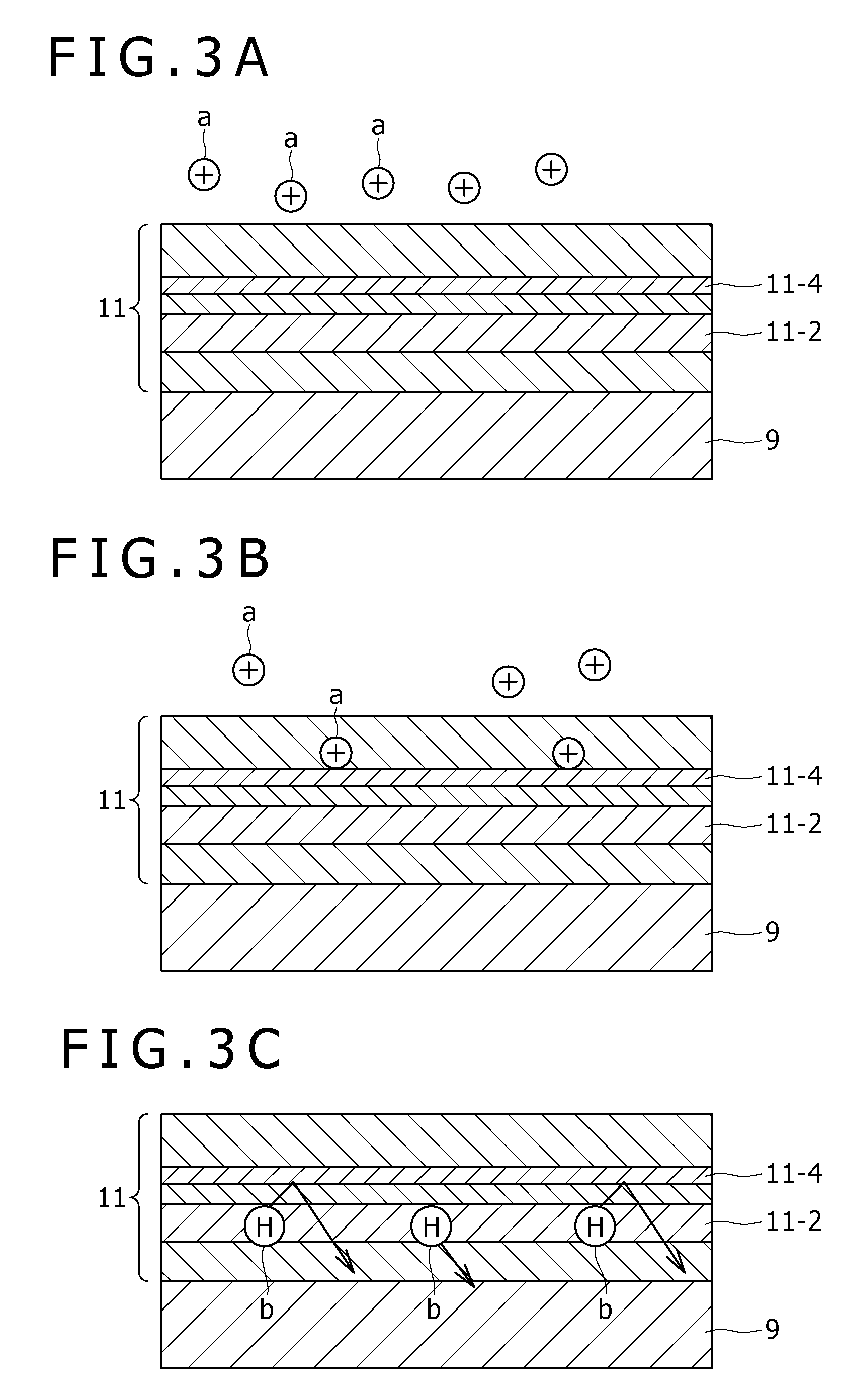
[0047]Specifically, the interlayer insulating film 11′ of the second embodiment has a four-layer structure in which a blocking silicon nitride film 11-4 is deposited directly on a hydrogen-containing silicon nitride film 11-2. This four-layer structure is obtained by sequentially depositing a lower silicon oxide film 11-1, the hydrogen-containing silicon nitride film 11-2, the blocking silicon nitride film 11-4, and an upper silicon oxide film 11-5 in that order from the semiconductor thin film side.

[0048]The detailed structures of the respective films are the same as those of the first embodiment.

[0049]Similarly to the first embodiment, a thin film semicond...


PUM


Abstract

The present invention is to provide a thin film semiconductor device including a semiconductor thin film and an interlayer insulating film configured to cover the semiconductor thin film. In the interlayer insulating film, a hydrogen supply part and a blocking part against contamination are deposited in that order from a semiconductor thin film side.

Description

CROSS REFERENCES TO RELATED APPLICATIONS[0001]The present invention contains subject matter related to Japanese Patent Application JP 2006-266301 filed in the Japan Patent Office on Sep. 29, 2006, the entire contents of which being incorporated herein by reference.BACKGROUND OF THE INVENTION[0002]1. Field of the Invention[0003]The present invention relates to a thin film semiconductor device, display, and method for manufacturing a thin film semiconductor device, and particularly to a thin film semiconductor device preferably used as a thin film transistor that employs a polycrystalline silicon film arising from crystallization by laser annealing, display employing the same, and method for manufacturing a thin film semiconductor device.[0004]2. Description of the Related Art[0005]In a flat-panel display such as a liquid crystal display and organic EL display, thin film transistors (TFTs) are provided as elements for driving pixel electrodes. Of the TFTs, a polycrystalline silicon TF...

Claims


Application Information

Patent Timeline
Patent Type & Authority Applications(United States)
IPC IPC(8): H01L29/04H01L21/20
CPCH01L27/1248H01L29/66765H01L27/1214
Inventor MORITA, HIROAKISHIOTANI, TOMOHIROKUBOTA, SHINJIABE, KAORU
Owner SONY CORP
Why Eureka
Try Eureka