Insulated gate semiconductor device

a technology of semiconductor devices and gate elements, which is applied in the direction of semiconductor devices, electrical equipment, transistors, etc., can solve the problems of limiting the minimum chip size, damage to the chip, and breakdown of the chip, and achieves high emitter ballast resistance and high resistance to electrical breakdown

Active Publication Date: 2008-04-03
MITSUBISHI ELECTRIC CORP
View PDF6 Cites 15 Cited by
  • Summary
  • Abstract
  • Description
  • Claims
  • Application Information

AI Technical Summary

Benefits of technology

[0023]The present invention has been devised to solve the above problems. It is, therefore, an object of the present invention to provide an insulated gate semicon...

Problems solved by technology

Before the IGBTs with a trench gate structure were developed, the minimum chip size was primarily limited by the amount of heat generated by the IGBTs when they were operated.
If the saturation current of an IGBT is too high, the IGBT generates a large amount of heat (equal to the time integral of the product of the saturation current and the collector-emitter voltage of the IGBT) when it is short-circuited, which might result in breakdown of the chip in a short time.
As a result, the short-circuit current continues to flow for a long time, resulting in damage to the chip due to the generated heat.
Furthermore, the ballast resistance prevents the saturation current from increasing to an unacceptably high level, sinc...

Method used


Image

  • Insulated gate semiconductor device
  • Insulated gate semiconductor device
  • Insulated gate semiconductor device

Examples


first embodiment

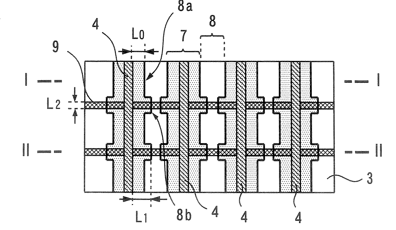
[0079]A description will now be made of an insulated gate semiconductor device according to a first embodiment of the present invention. This semiconductor device includes: an insulated gate bipolar transistor(s), or IGBT(s), having a trench gate structure; and an n-type semiconductor substrate having a first principal surface (or top principal surface) and a second principal surface (or back principal surface). FIG. 1 is a plan view of this semiconductor device as viewed from the first principal surface side of the semiconductor substrate. FIGS. 2 and 3 are cross-sectional views taken along lines I-I and II-II, respectively, of FIG. 1.

[0080]Referring to FIGS. 2 and 3, a base layer 3 containing a p-type impurity is provided adjacent to the first principal surface of the semiconductor substrate 2. A plurality of trenches 4 are formed so as to penetrate through the base layer 3 and into the first principal surface of the semiconductor substrate 2.

[0081]These trenches (or trench openin...

second embodiment

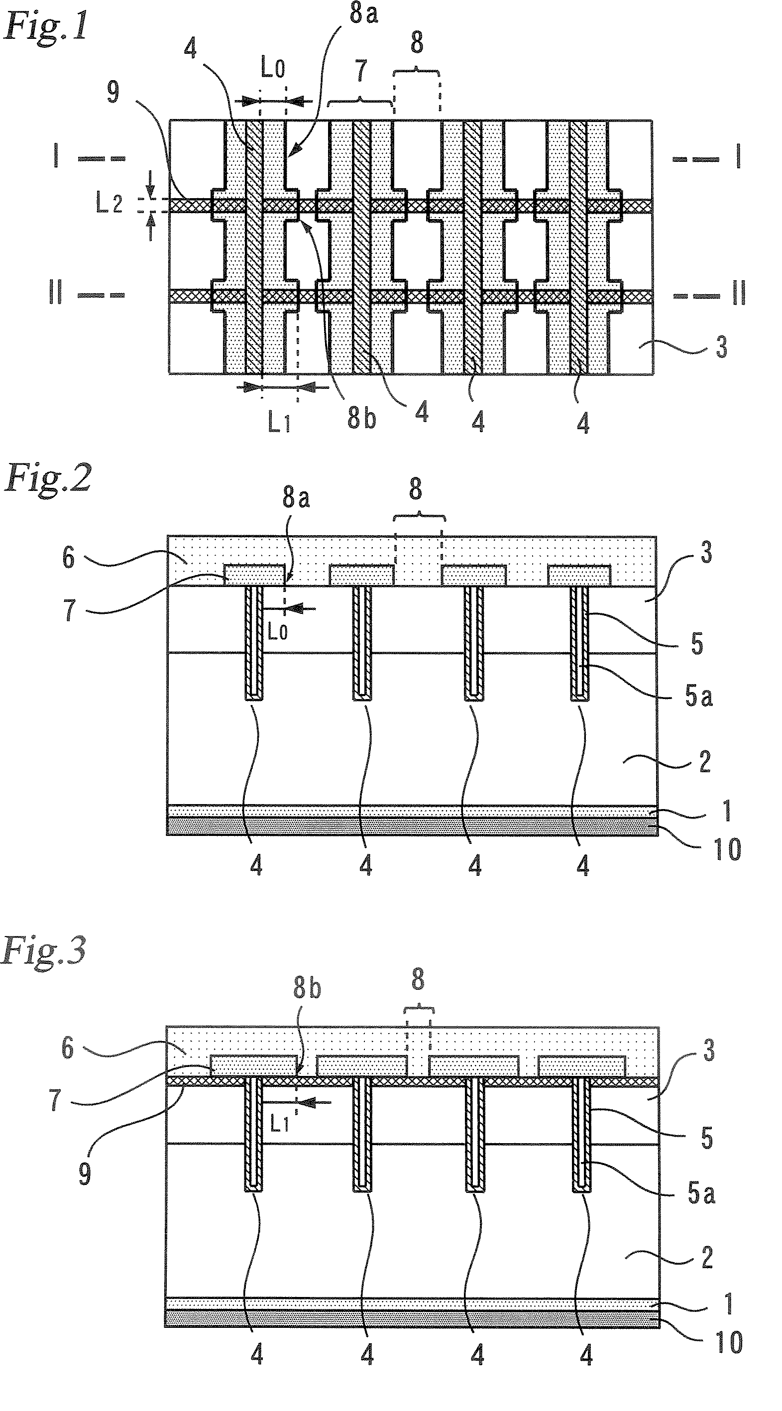
[0097]A description will now be made of an insulated gate semiconductor device according to a second embodiment of the present invention with reference to FIGS. 7 to 9. The following description will focus on the differences from the first embodiment. FIG. 7 is a plan view of the insulated gate semiconductor device according to this embodiment. FIGS. 8 and 9 are cross-sectional views taken along lines I-I and II-II respectively, of FIG. 7.

[0098]Referring to FIG. 7, a plurality of trenches 4 are arranged in stripes, and a dummy trench 4a is provided between each two adjacent trenches 4 so as to extend in the longitudinal direction of the trenches 4. Thus, these dummy trenches 4a are arranged in stripes and extend in the longitudinal direction of the trenches 4. Further, first emitter diffusion layers 9 are formed so as to extend in a direction intersecting the trenches 4 and connect between the trenches 4 and the dummy trenches 4a. More specifically, the dummy trenches 4a are formed ...

third embodiment

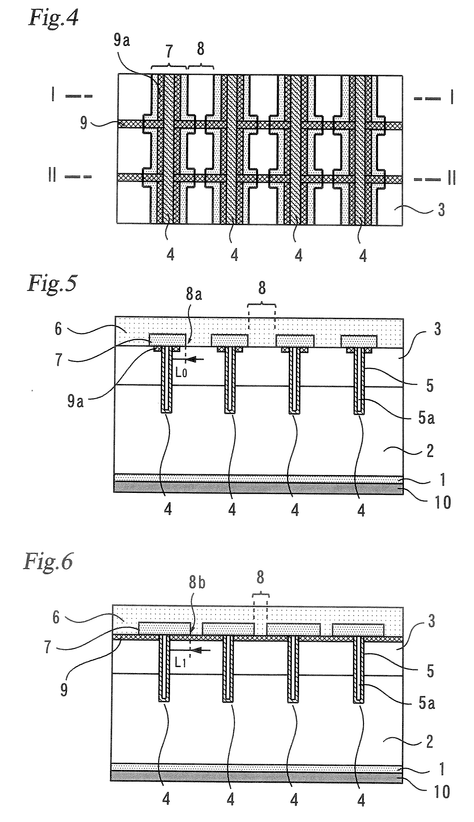
[0116]A description will now be made of an insulated gate semiconductor device according to a third embodiment of the present invention with reference to FIGS. 28 to 31. The following description will focus on the differences from the second embodiment. FIG. 28 is a plan view of the insulated gate semiconductor device according to this embodiment FIGS. 29 to 31 are cross-sectional views taken along lines I-I, II-II, and III-III, respectively, of FIG. 28.

[0117]Referring to FIG. 28, a plurality of trenches 4 are arranged in stripes, and a dummy trench 4a is provided between each two adjacent trenches 4. Further, second emitter diffusion layers 9a having a strip shape are provided in contact with respective sides of each trench 4 and connected to one end of their respective first emitter diffusion layers 9, as shown in FIGS. 28 and 31. The first emitter diffusion layers 9 and the second emitter diffusion layers 9a together form T-shaped emitter diffusion layers. All other components an...


PUM


Abstract

An IGBT comprises trenches arranged in strips, first emitter diffusion layers formed so as to extend in a direction intersecting the trenches, and contact regions formed to have a rectangular shape. The portions of the contact regions on the first emitter diffusion layers have a smaller width than the other portions, the width extending in the direction intersecting the trenches. This configuration allows for an increase in the emitter ballast resistance of the emitter diffusion layers, resulting in enhanced resistance to electrical breakdown due to short circuit.

Description

BACKGROUND OF THE INVENTION [0001]1. Field of the Invention[0002]The present invention relates to an insulated gate semiconductor device, and more particularly to an insulated gate semiconductor device adapted to exhibit reduced variation in saturation current and increased resistance to electrical breakdown in a short-circuit capacity test.[0003]2. Background Art[0004]IGBTs (Insulated Gate Bipolar Transistors), which are a type of insulated gate semiconductor device, are widely used in power converters such as inverters, since they combine the high speed operation of MOSFETs and the low turn-on voltage characteristics of bipolar transistors.[0005]In recent years, the turn-on voltage and the switching loss of transistors have been reduced due to development of IGBTs having a trench gate structure. Furthermore, with the appearance of improved IGBTs and IEGTs (Injection Enhanced Gate transistors) having a carrier storage layer, the longitudinal carrier distribution within the chip can...

Claims


Application Information

Patent Timeline
IPC IPC(8): H01L29/94
CPCH01L29/0696H01L29/7397H01L29/66348
Inventor HAMAGUCHI, TAKUYAHARUGUCHI, HIDEKITSUNODA, TETSUJIRO
Owner MITSUBISHI ELECTRIC CORP
Why Eureka
Try Eureka