Cap Wafer for Wafer Bonded Packaging and Method for Manufacturing the Same

a technology of cap wafer and packaging, which is applied in the direction of semiconductor devices, microelectromechanical systems, semiconductor/solid-state device details, etc., can solve the problems of high production cost, high production cost, and the inability to meet the requirements of plating technique, and achieve the effect of reducing the cost of copper filling and copper filling, and reducing the cost of production

Inactive Publication Date: 2008-04-03
PHOCO
View PDF12 Cites 177 Cited by
  • Summary
  • Abstract
  • Description
  • Claims
  • Application Information

AI Technical Summary

Problems solved by technology

However, deep reactive ion etching and copper-filling processes are known as most costly among the semiconductor fabrication processes, and moreover copper-filling that is typically performed by plating technique requires very long process time.
However, such conventional through-hole interconnection method is problematic in that SOI wafer, which is more expensive than general silicon wafer, is required and due to the complexity for forming interconnection in the presence of already formed through-holes which penetrate the top and bottom sides of the wafer, it accompanies a disadvantage that production cost is high to exceed the savings expected from replacing deep reactive ion etching.

Method used


Image

  • Cap Wafer for Wafer Bonded Packaging and Method for Manufacturing the Same
  • Cap Wafer for Wafer Bonded Packaging and Method for Manufacturing the Same
  • Cap Wafer for Wafer Bonded Packaging and Method for Manufacturing the Same

Examples


Embodiment Construction

[0026] Hereinafter, preferred examples of the present invention will be provided so that those skilled in the art can easily carry out the present invention.

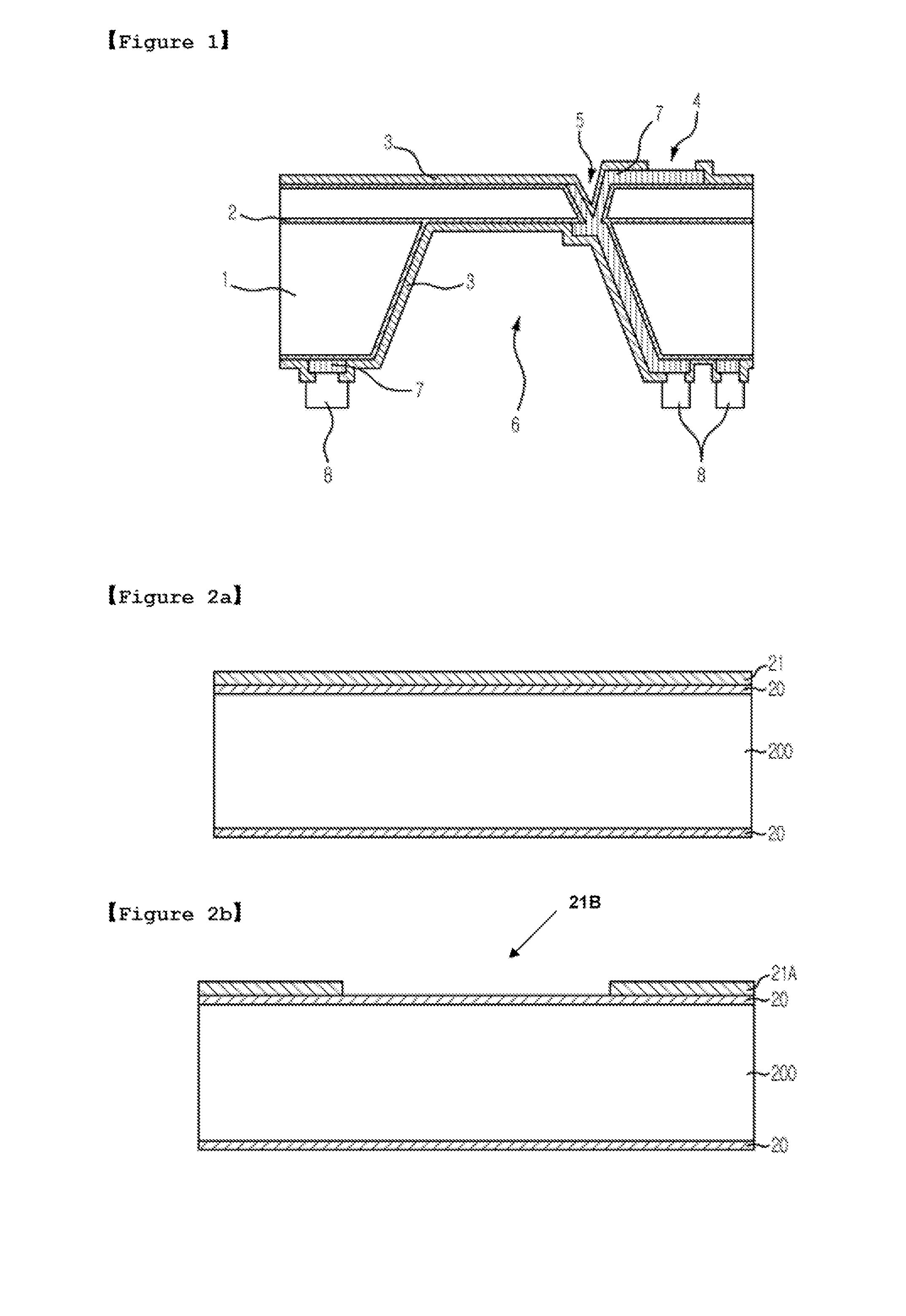
[0027]FIGS. 2a to 2k are flowcharts showing steps of a method for fabricating silicon cap wafers according to one example of the present invention.

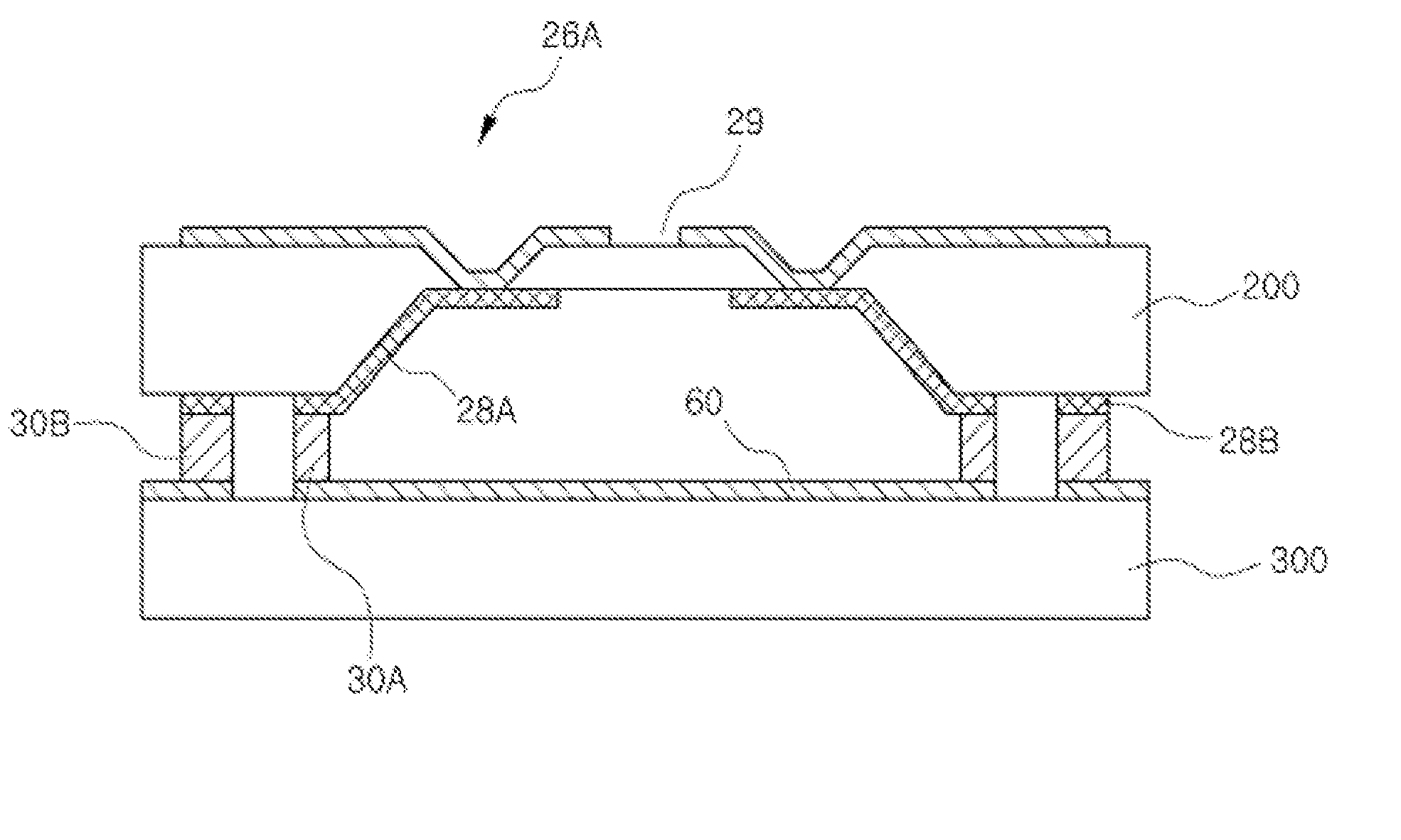
[0028] The wafer level packaging process according to one example of the present invention comprises steps of depositing an etch mask layer (20) on the top and bottom sides of a silicon wafer (200) having (100) crystal plane and coating photoresist (21) on the top side of the silicon wafer (200), as shown in FIG. 2a. For the etch mask layer (20), it is preferred to use silicon oxide layer, silicon nitride layer or stacked layer of silicon oxide layer and silicon nitride layer.

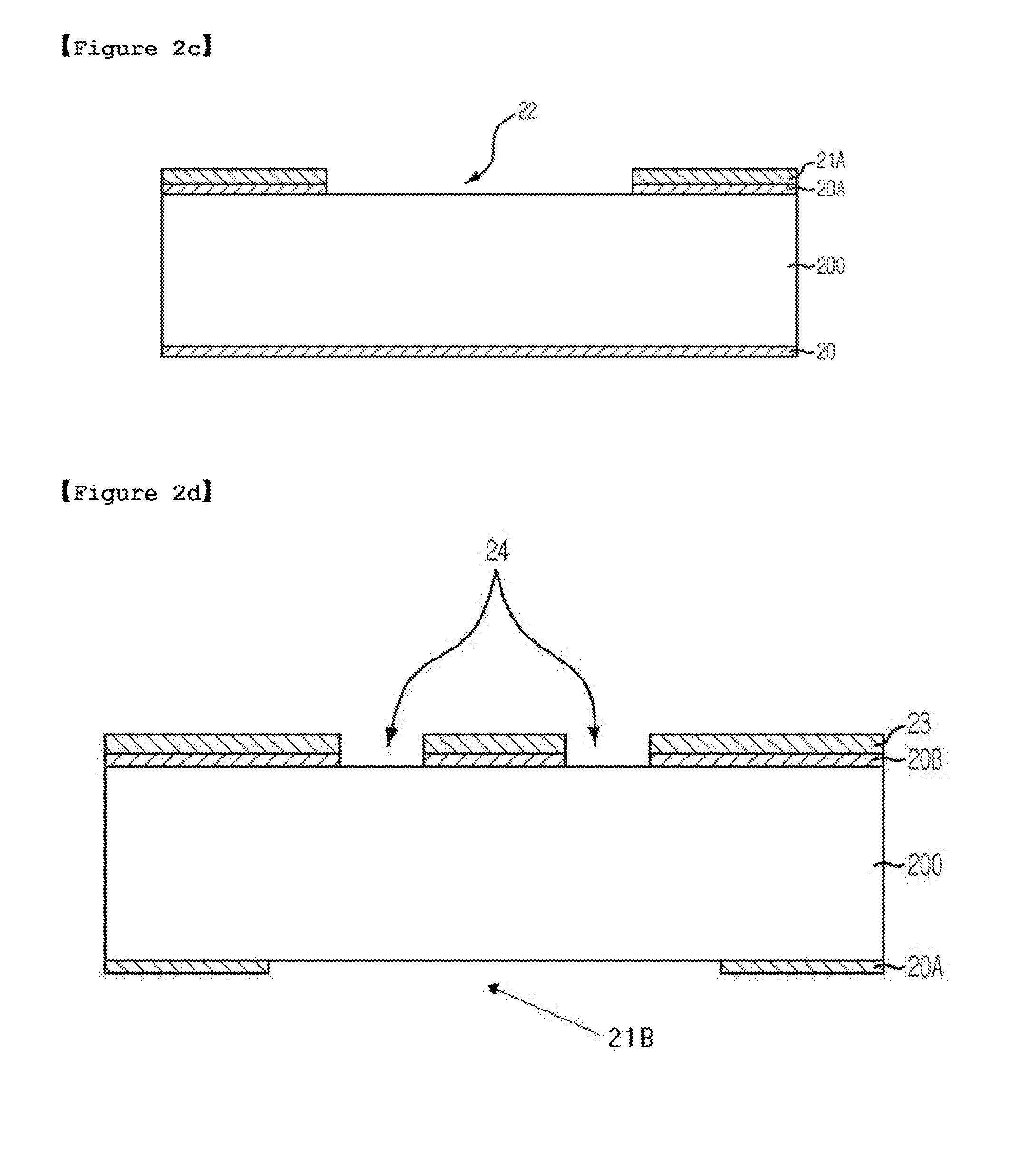
[0029] Subsequently, as shown in FIG. 2b, cavity etch window (21B) is defined by selectively removing the photoresist (21A) on the cavity etch window by using photolithography techniques.

[0030] Next, as shown...


PUM


Abstract

The present invention relates to semiconductor device manufacturing techniques, and specifically to a field of device packaging techniques at wafer level. More specifically, it relates to a cap wafer for wafer bonding application that is bonded to top part of a device wafer. The method of the present invention excludes the use of deep reactive ion etching of silicon to form a through silicon via. The present invention provides a method for the preparation of cap wafer for wafer bonding application with a simple process of through silicon via interconnection and a wafer level packaging method using the same.

Description

TECHNICAL FIELD [0001] The present invention relates to semiconductor device manufacturing techniques, and specifically to a field of wafer level packaging techniques. More specifically, it relates to a cap wafer for wafer bonded hermetic packaging that is bonded to top of device wafer. BACKGROUND ART [0002] Wafer level Packaging of semiconductor device by wafer bonding is a batch, mass-production method which from hundreds to thousands of devices are packaged simultaneously. Therefore, it is advantageous in that packaging cost can be reduced. Wafer level packaging using wafer bonding can be categorized into the one for general integrated circuit devices such as memory devices, etc. and the other for sensor / MEMS (Microelectromechanical Systems) having sensing element or mechanically moving structure on the surface of device. [0003] For general IC field, the major object of wafer bonding technique is to stack chips three-dimensionally, thus it is mainly used for increasing the integr...

Claims


Application Information

Patent Timeline
Patent Type & Authority Applications(United States)
IPC IPC(8): H01L21/00
CPCB81B2203/0384B81B2207/097B81C1/00301H01L21/76898H01L23/10H01L2924/0002H01L2924/01079H01L2924/00H01L23/02H01L23/04
Inventor LEE, SANG-HWANRYU, YEON-DUCKAN, JAE-YONGCHOI, HYUN-JINSHIN, MYOUNG-SEON
Owner PHOCO
Why Eureka
Try Eureka