Substrate processing apparatus and substrate processing method

a substrate processing and substrate technology, applied in the direction of grinding machine components, manufacturing tools, lapping machines, etc., can solve the problems of easy corrosion, copper wiring may become electrically unstable, corrosion cannot be completely prevented, etc., to prevent continuous wiring corrosion, prevent corrosion on the wiring, and prevent corrosion.

Inactive Publication Date: 2008-04-03
PANASONIC CORP
View PDF8 Cites 21 Cited by
  • Summary
  • Abstract
  • Description
  • Claims
  • Application Information

AI Technical Summary

Benefits of technology

[0016]As a result of analyzing this phenomenon, the present inventors discovered the following. The copper wirings before the completion of the final stage polishing in the CMP processing are electrically connected via the metal remaining on the wafer surface (Here, a copper film, barrier metal and adhesion layer). In the meantime, the copper wirings where the final stage polishing has been completed have no metal film on the wafer surface and they are electrically disconnected, respectively. In other words, electrically-floating copper wirings exist in the completely polished copper wirings. Consequently, the copper wirings may become electrically unstable, and corrosion easily occurs.
[0031]With the present invention, a time period to attach the object to be processed where the final stage of polishing has been completed to ultrapure water can be predetermined. As a result, a yield reduction that increases associated with an increase of the attachment time to the ultrapure water can be restrained. Further, even if the ultrapure water attachment time exceeds the predetermined time period, continuous yield reduction can be prevented.

Problems solved by technology

However, even when the technology disclosed in Japanese Unexamined Patent Application Publications 2002-93760 or 2005-109094 is applied, the corrosion of the copper wiring cannot completely be prevented. FIG. 11 is a graph showing the relationship between an elapsed time after the completion of the final stage of polishing and a production yield.
Consequently, the copper wirings may become electrically unstable, and corrosion easily occurs.

Method used


Image

  • Substrate processing apparatus and substrate processing method
  • Substrate processing apparatus and substrate processing method
  • Substrate processing apparatus and substrate processing method

Examples


first embodiment

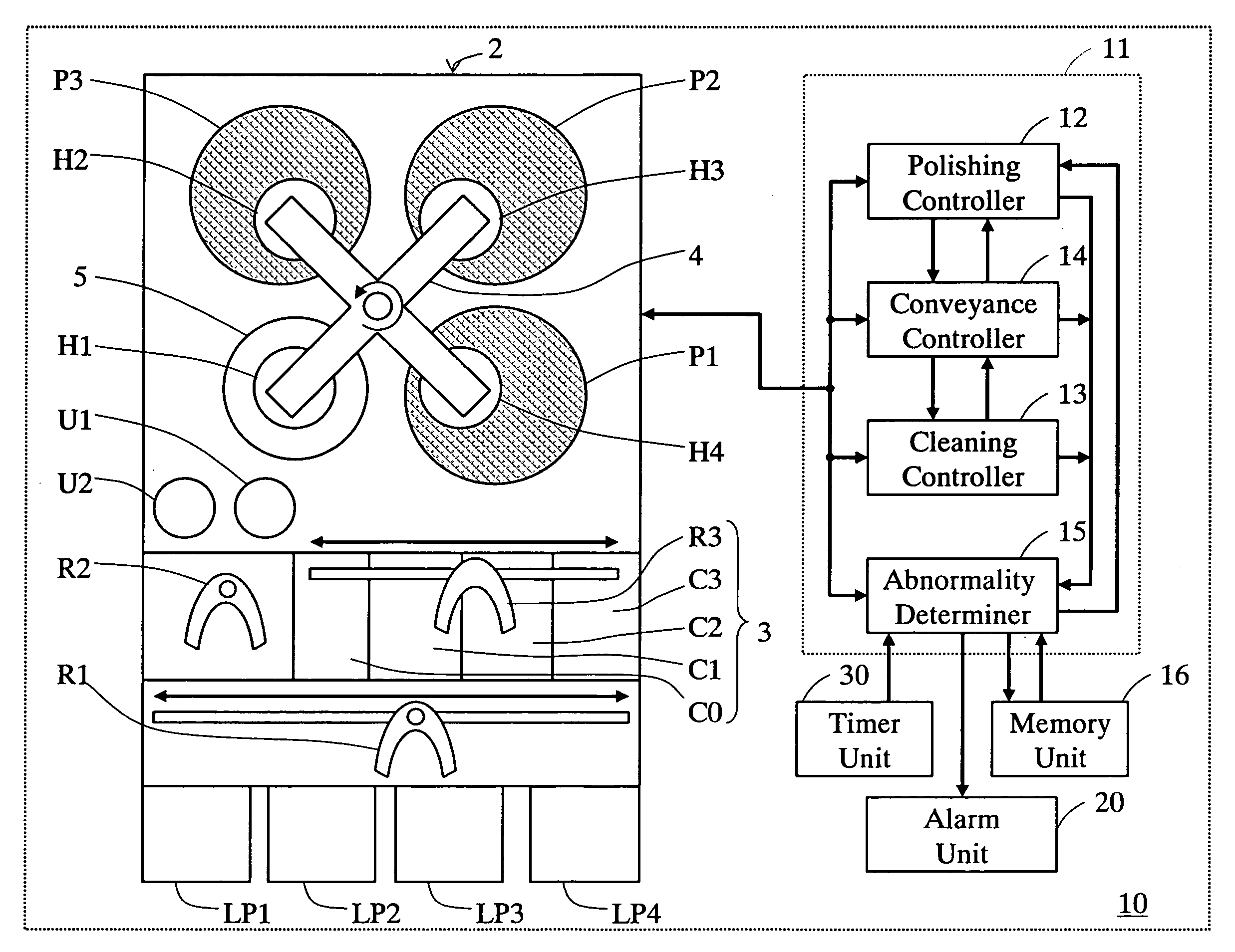
[0046]FIG. 1 is a schematic block diagram showing the substrate processing apparatus in the first embodiment relating to the present invention. As shown in FIG. 1, a substrate processing apparatus 10 in the present embodiment includes a polishing section 2 that polishes wafers and a cleaning section 3 that cleans the wafers polished by the polishing section 2. The cleaning section 3 is arranged adjacent to the polishing section 2, and a wet robot R2 that conveys the wafers is arranged at the position adjacent to both of the polishing section 2 and the cleaning section 3. Further, a dry robot R1 that is movable along the wet robot R2 and the cleaning section 3 is arranged at the position, which is the opposite side from the polishing section 2, across the cleaning section 3 and the wet robot R2. In addition, multiple load ports LP1, LP2, LP3 and LP4 where containers, such as FOUP (front opening unified pod), containing the wafers, are detachably arranged in positions which are on the...

second embodiment

[0098]In the first embodiment, because a wafer is conveyed from the polishing section 2 to the cleaning section 3 without any conveyance reserve, the wafer conveyance time period is a bare essential time period, and corrosion of the copper wiring is prevented. However, as shown in FIG. 11, if it is configured that the cleaning processing of a wafer where the final stage polishing has been completed can be started within a predetermined time period (for example, 300 seconds), wiring corrosion caused by attachment of ultrapure water can be restrained. Then, in the present embodiment, a substrate processing apparatus where the conveyance time period from the polishing section 2 to the cleaning section 3 can be kept within a predetermined time is described.

[0099]FIG. 4 is a schematic block diagram showing the substrate processing apparatus in the second embodiment relating to the present invention. As shown in FIG. 4, a substrate processing apparatus 40 of the present invention polishes...

third embodiment

[0118]In the second embodiment, it is configured that an expected polishing completion time by polishing plane for the final stage polishing and expected polishing completion times by the other polishing platens do not satisfy a pre-set allowed range, respectively, the polishing is stopped. However, when they do not satisfy the pre-set allowed range, another configuration where an expected polishing completion time is adjusted can also be adopted. Then, in the present embodiment, a configuration where polishing conditions for the polishing platens may be changed according to an expected polishing completion time for the polishing platens, respectively, is described.

[0119]FIG. 6 is a schematic block diagram showing a substrate processing apparatus in the third embodiment relating to the present invention. As shown in FIG. 6, a substrate processing apparatus 60 in the present embodiment polishes wafers using three platens, as similar to the substrate processing apparatuses 10 and 40 d...


PUM

PropertyMeasurementUnit
timeaaaaaaaaaa
completion timeaaaaaaaaaa
time periodaaaaaaaaaa

Abstract

The substrate processing apparatus relating to the present invention comprises a polishing section where wafers are sequentially arranged, and that has multiple polishing platens for polishing a metal film on the wafer surface in stages. The wafers are simultaneously conveyed between the polishing platens by a rotating head mechanism. Further, the wafers polished by the polishing platen for the final stage polishing are sequentially conveyed to a cleaning section and are cleaned. The wafers from the polishing section to the cleaning section are conveyed by a load-unload unit, a post-polishing wafer reversal unit and wet robots. Then, the operation of each part is controlled by an apparatus controller to start the cleaning processing of the polished wafers by the polishing platen for the final stage polishing within a predetermined time period from the completion of polishing by the polishing platen for the final stage polishing. With this control, corrosion to wiring containing corrodible metal, such as copper, can be assuredly prevented.

Description

CROSS-REFERENCE TO RELATED APPLICATION[0001]The present application claims the benefit of patent application number 2006-271983, filed in Japan on Oct. 3, 2006, the subject matter of which is incorporated herein by reference.BACKGROUND OF THE INVENTION[0002]1. Field of the Invention[0003]The present invention relates to a substrate processing apparatus and a substrate processing method, and particularly relates to a technology for preventing surface abnormalities and corrosion in metal wiring from being formed using chemical mechanical polishing.[0004]2. Description of the Related Art[0005]Metal wiring is widely used as wiring to compose a semiconductor integrated circuit device (hereafter, referred to as a semiconductor device). Conventionally, the metal wiring has been formed by means of a metal film deposited onto a silicon substrate (wafer) with the application of lithography technology and etching technology. This type of metal film includes aluminum (Al) alloy film and tungste...

Claims


Application Information

Patent Timeline
Patent Type & Authority Applications(United States)
IPC IPC(8): B24B7/19B24B37/04H01L21/304
CPCH01L21/67219B24B37/345H01L21/304H01L21/02
Inventor SATO, NAOAKIIMAI, SHINICHI
Owner PANASONIC CORP
Why Eureka
Try Eureka